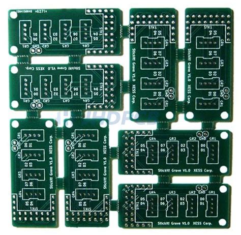
What is PCB Panelization?
PCB panelization is the process of arranging multiple identical or different PCB designs on a single larger board, known as a panel. The primary purpose of panelization is to optimize the manufacturing process by maximizing the number of PCBs produced per panel, reducing material waste, and improving overall efficiency.
Benefits of PCB Panelization
- Cost reduction: By producing multiple PCBs on a single panel, the manufacturing costs per board are significantly reduced.
- Improved efficiency: Panelization allows for faster fabrication and assembly, as multiple boards can be processed simultaneously.
- Consistent quality: Panelizing PCBs ensures consistent quality across all boards in the panel, as they are subjected to the same manufacturing conditions.
Key Considerations for PCB Panelization Design
When designing PCBs for panelization, there are several key factors to consider to ensure optimal results:
1. Panel Size and Material
The choice of panel size and material depends on the specific requirements of your PCB project. Standard panel sizes vary depending on the manufacturer, but common sizes include:
| Panel Size (mm) | Panel Size (inches) |
|---|---|
| 228.6 x 304.8 | 9 x 12 |
| 304.8 x 457.2 | 12 x 18 |
| 457.2 x 609.6 | 18 x 24 |
The most commonly used materials for PCB panels are:
- FR-4: A flame-retardant glass-reinforced epoxy laminate, suitable for most applications.
- Aluminum: Used for heat dissipation and high-power applications.
- Polyimide: Ideal for flexible PCBs and high-temperature applications.
2. Board Spacing and Clearance
Proper spacing between individual PCBs on the panel is crucial to ensure clean and accurate separation during the depaneling process. The minimum spacing between boards depends on the depaneling method used:
| Depaneling Method | Minimum Spacing |
|---|---|
| V-Scoring | 1.0 mm |
| Tab Routing | 1.5 mm |
| Perforated | 2.0 mm |
Additionally, maintain a minimum clearance of 3-5 mm between the edge of the panel and the outermost PCBs to avoid damage during handling and processing.
3. Fiducial Markers and Tooling Holes
Fiducial markers and tooling holes are essential for accurate alignment and registration during the manufacturing process.
- Fiducial markers: Place at least three fiducial markers on the panel, preferably near the corners, to ensure precise alignment during solder paste application, component placement, and inspection.
- Tooling holes: Include tooling holes on the panel to help secure the panel during fabrication and assembly. Typical tooling hole diameters range from 2.5 mm to 5 mm.
4. Depaneling Methods
There are several methods for separating individual PCBs from the panel, each with its advantages and limitations:
- V-Scoring: A V-shaped groove is cut along the board edges, allowing for easy snap-off separation. This method is cost-effective but may cause stress on the PCB edges.
- Tab Routing: Small tabs are left connecting the boards, which are later broken off. This method provides cleaner edges but may require manual separation.
- Perforated: A series of closely spaced holes are drilled along the board edges, allowing for snap-off separation. This method is suitable for thicker PCBs but may leave rough edges.
- Milling/Routing: A milling or routing tool is used to cut the boards from the panel. This method provides clean, smooth edges but is more expensive and time-consuming.
Consider the specific requirements of your PCB, such as edge quality, depaneling speed, and cost, when selecting the appropriate depaneling method.
5. Panelization Layout and Orientation
When arranging PCBs on the panel, consider the following layout and orientation guidelines:
- Optimize panel utilization by minimizing waste material between boards.
- Orient the boards to minimize the overall panel size and maximize the number of boards per panel.
- Ensure that the board orientation is consistent with the assembly process, such as pick-and-place machine requirements.
- If using mixed designs on a single panel, group similar designs together to simplify the assembly process.
6. Solder Mask and Silkscreen
Solder mask and silkscreen considerations for panelized PCBs include:
- Extend the solder mask and silkscreen beyond the individual board edges to provide protection and identification during the depaneling process.
- Ensure that the solder mask and silkscreen apertures are sized appropriately to prevent peeling or damage during depaneling.
- Include panel-level markings, such as panel identification, revision numbers, and assembly instructions, to aid in the manufacturing process.
7. Testing and Inspection
Incorporate testing and inspection considerations into your panelization design:
- Include test coupons or bare board test points on the panel to facilitate electrical testing and quality control.
- Provide sufficient clearance around test points to allow for probing and inspection.
- Consider adding panel-level fiducial markers or barcodes to enable automated optical inspection (AOI) and traceability.

Frequently Asked Questions (FAQ)
- What is the minimum board spacing required for V-Scoring depaneling?
-
The minimum board spacing for V-Scoring depaneling is typically 1.0 mm.
-
Can different PCB designs be panelized together?
-
Yes, different PCB designs can be panelized together on a single panel. However, it is important to group similar designs and consider the assembly process requirements when arranging the boards.
-
What are fiducial markers, and why are they important?
-
Fiducial markers are reference points on the PCB panel that help ensure precise alignment during solder paste application, component placement, and inspection. They are typically placed near the corners of the panel.
-
How do I choose the appropriate depaneling method for my PCB project?
-
The choice of depaneling method depends on factors such as edge quality requirements, depaneling speed, PCB Thickness, and cost. Consider the specific needs of your project and consult with your manufacturer to determine the most suitable method.
-
Can solder mask and silkscreen be extended beyond the individual board edges on a panelized PCB?
- Yes, extending the solder mask and silkscreen beyond the individual board edges is recommended to provide protection and identification during the depaneling process. Ensure that the apertures are sized appropriately to prevent peeling or damage.

Conclusion
PCB panelization is a vital aspect of PCB manufacturing that enables efficient fabrication and assembly of multiple boards on a single panel. By understanding and following the key design guidelines discussed in this article, you can optimize your PCB panelization process, reduce costs, and improve overall quality. Remember to consider factors such as panel size and material, board spacing and clearance, fiducial markers and tooling holes, depaneling methods, layout and orientation, solder mask and silkscreen, and testing and inspection when designing your panelized PCBs. By working closely with your PCB manufacturer and adhering to these guidelines, you can ensure the success of your PCB projects and achieve the best possible results.


Leave a Reply