What is Back Drill in PCB?
Back drill, also known as controlled depth drilling, is a PCB manufacturing process used to remove the stub left in through-holes after drilling Multilayer PCBs. By removing the unwanted portion of the plated through-hole, back drilling improves signal integrity, reduces capacitance and inductance, and helps maintain the impedance of high-speed signals.
In a typical multilayer PCB, a through-hole is drilled and plated through the entire board thickness, even if the signal only needs to connect to one or a few layers. This creates an unnecessary stub that can cause signal reflections and degrade signal quality, especially at high frequencies.
Back drilling precisely removes the unwanted plating in the through-hole up to a specific depth, leaving only the necessary connections intact. This process is critical for high-speed PCB designs, such as those used in telecommunications, networking, and high-performance computing.
How Does Back Drilling Work?
The back drilling process involves the following steps:
-
Primary Drilling: First, the primary through-holes are drilled and plated through the entire thickness of the PCB.
-
Back Drill Programming: The PCB design software generates the back drill file, which specifies the location and depth of each back drill.
-
Alignment: The PCB is aligned on the drilling machine using Fiducial Marks to ensure precise positioning.
-
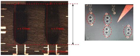
Controlled Depth Drilling: A specialized drill bit, typically a high-speed steel or carbide drill, is used to remove the unwanted plating up to the specified depth. The depth is carefully controlled to avoid damaging the necessary connections.
-
Cleaning: After back drilling, the PCB is cleaned to remove any debris generated during the process.

Advantages of Back Drilling PCBs
Back drilling offers several advantages for high-speed PCB designs:
-
Improved Signal Integrity: By removing the unwanted stub, back drilling reduces signal reflections and distortion, improving overall signal integrity.
-
Reduced Capacitance and Inductance: The removal of the stub decreases the capacitance and inductance associated with the through-hole, which can improve signal quality and timing.
-
Impedance Control: Back drilling helps maintain the characteristic impedance of high-speed signals by removing the discontinuity caused by the stub.
-
Higher Bandwidth: With improved signal integrity, back drilled PCBs can support higher bandwidth and data rates.
-
Compatibility with High-Frequency Applications: Back drilling enables PCBs to be used in high-frequency applications, such as 5G telecommunications, high-speed networking, and advanced computing systems.

Considerations for Back Drilling PCBs
When implementing back drilling in your PCB design, consider the following factors:
-
Design for Manufacturability: Ensure your PCB design is compatible with the back drilling process. Provide clear specifications for the location and depth of each back drill, and consider the limitations of the drilling equipment.
-
Material Selection: Choose PCB materials that can withstand the back drilling process without delamination or other damage. High-quality, reinforced materials are recommended for back drilled PCBs.
-
Drill Bit Selection: Select the appropriate drill bit for back drilling based on the PCB material, thickness, and required hole size. High-speed steel and carbide drills are commonly used for back drilling.
-
Depth Control: Accurately control the depth of the back drill to avoid damaging the necessary connections. Use precise depth control methods, such as laser measurement or depth-controlled drilling machines.
-
Cleaning and Inspection: After back drilling, thoroughly clean the PCB to remove any debris, and inspect the back drilled holes to ensure they meet the specified depth and quality requirements.

FAQs
1. What is the difference between back drilling and normal drilling in PCBs?
Normal drilling creates through-holes that are plated through the entire thickness of the PCB, even if the signal only needs to connect to a few layers. Back drilling, on the other hand, removes the unwanted plating up to a specific depth, leaving only the necessary connections intact.
2. Is back drilling necessary for all PCB designs?
No, back drilling is primarily used in high-speed PCB designs where signal integrity is critical. It is particularly important for applications such as telecommunications, networking, and high-performance computing, where high frequencies and fast data rates are involved.
3. How does back drilling improve signal integrity?
Back drilling improves signal integrity by removing the unwanted stub in the through-hole. The stub can cause signal reflections and distortion, degrading signal quality. By removing the stub, back drilling reduces these issues and helps maintain the characteristic impedance of the signal.
4. What materials are suitable for back drilled PCBs?
High-quality, reinforced PCB materials that can withstand the back drilling process without delamination or other damage are recommended for back drilled PCBs. Examples include FR-4, high-Tg FR-4, and polyimide materials.
5. How is the depth of the back drill controlled?
The depth of the back drill is controlled using precise depth control methods, such as laser measurement or depth-controlled drilling machines. The PCB design software generates a back drill file that specifies the location and depth of each back drill, ensuring accurate and consistent results.
Conclusion
Back drilling is a crucial process in the manufacturing of high-speed PCBs, enabling improved signal integrity, reduced capacitance and inductance, and better impedance control. By removing the unwanted stub in plated through-holes, back drilling allows PCBs to support higher bandwidths and data rates, making them suitable for demanding applications in telecommunications, networking, and high-performance computing.
When designing PCBs that require back drilling, it is essential to consider factors such as design for manufacturability, material selection, drill bit choice, depth control, and proper cleaning and inspection. By carefully addressing these aspects, you can ensure that your back drilled PCBs meet the highest quality standards and perform optimally in high-speed applications.
As technology continues to advance and the demand for faster, more reliable electronic systems grows, the importance of back drilling in PCB manufacturing will only increase. By understanding the principles and best practices of back drilling, PCB designers and manufacturers can stay at the forefront of this essential technique and create PCBs that push the boundaries of performance and innovation.
| Aspect | Normal Drilling | Back Drilling |
|---|---|---|
| Plating | Through entire PCB Thickness | Removed up to a specific depth |
| Signal Integrity | May degrade due to stub | Improved by removing stub |
| Capacitance & Inductance | Higher due to stub | Reduced by removing stub |
| Impedance Control | Discontinuity caused by stub | Maintained by removing stub |
| High-Frequency Compatibility | Limited | Enhanced |
Table 1: Comparison of normal drilling and back drilling in PCBs


Leave a Reply