Introduction to SMT Stencils and PCB prototyping
Surface Mount Technology (SMT) has revolutionized the electronics manufacturing industry by enabling the production of smaller, faster, and more efficient printed circuit boards (PCBs). One of the key components in the SMT process is the stencil, which plays a crucial role in simplifying the PCB prototyping process. SMT stencils are thin metal sheets with precisely cut apertures that allow for the accurate application of solder paste onto the PCB pads.
PCB prototyping is an essential step in the development of new electronic devices, as it allows engineers to test and refine their designs before committing to full-scale production. However, the prototyping process can be time-consuming and costly, especially when dealing with complex PCB layouts. This is where SMT stencils come into play, offering a range of benefits that streamline the prototyping process and improve the overall quality of the final product.
In this article, we will explore the various aspects of SMT stencils and their impact on PCB prototyping. We will discuss the different types of SMT stencils, their manufacturing process, and the advantages they offer in terms of accuracy, consistency, and efficiency. Additionally, we will delve into the best practices for designing and utilizing SMT stencils to optimize the PCB prototyping process.
Understanding the Role of SMT Stencils in PCB Prototyping
What are SMT Stencils?
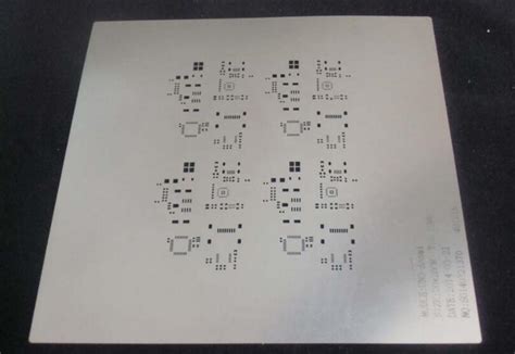
SMT stencils are thin metal sheets, typically made of stainless steel or nickel, that feature precisely cut apertures corresponding to the pads on a PCB. These apertures allow for the controlled application of solder paste onto the PCB pads, ensuring the correct amount of solder is deposited in the right locations.
The thickness of an SMT stencil can vary depending on the specific requirements of the PCB design, but it usually ranges from 0.1 mm to 0.2 mm (4 to 8 mils). The aperture sizes and shapes are carefully designed to match the dimensions of the PCB pads, taking into account factors such as the component package type, pad size, and pitch.
The Role of SMT Stencils in the PCB assembly Process
The PCB assembly process using SMT stencils typically involves the following steps:
-
Solder Paste Application: The stencil is aligned with the PCB, and solder paste is applied onto the stencil using a squeegee or automated solder paste printer. The solder paste is forced through the apertures, depositing the correct amount onto the PCB pads.
-
Component Placement: After the solder paste is applied, the PCB moves to the pick-and-place machine, where surface mount components are automatically placed onto the pads with high precision.
-
Reflow Soldering: The PCB with the placed components is then sent through a reflow oven, where the solder paste melts and forms a strong electro mechanical bond between the components and the PCB pads.
-
Inspection and Testing: Finally, the assembled PCB undergoes visual inspection and electrical testing to ensure proper functionality and quality.
SMT stencils play a critical role in the first step of this process, as they directly impact the accuracy and consistency of solder paste application. By using a well-designed SMT stencil, engineers can ensure that the right amount of solder paste is deposited onto the pads, minimizing defects such as bridging, insufficient solder, or solder balls.
Advantages of Using SMT Stencils in PCB Prototyping
Utilizing SMT stencils in PCB prototyping offers several key advantages:
-
Improved Accuracy: SMT stencils enable the precise application of solder paste onto the PCB pads, ensuring that the correct amount is deposited in the right locations. This accuracy is essential for achieving reliable solder joints and minimizing defects.
-
Increased Consistency: By using an SMT stencil, the solder paste application process becomes highly repeatable, resulting in consistent solder paste deposits across multiple PCBs. This consistency is particularly important in prototyping, where multiple iterations of a design may be required.
-
Enhanced Efficiency: SMT stencils streamline the solder paste application process, reducing the time and effort required compared to manual methods. This efficiency gain is especially valuable in prototyping, where quick turnaround times are often critical.
-
Cost Reduction: By minimizing defects and improving the overall quality of the assembled PCBs, SMT stencils help reduce costs associated with rework and scrap. Additionally, the increased efficiency offered by SMT stencils can lead to cost savings in terms of labor and materials.

Types of SMT Stencils and Their Manufacturing Process
Types of SMT Stencils
There are several types of SMT stencils available, each with its own unique characteristics and applications:
-
Laser-Cut Stencils: Laser-cut stencils are created using a high-precision laser to cut the apertures into the stencil material. This method offers excellent accuracy and can accommodate complex aperture shapes and fine pitch components. Laser-cut stencils are widely used in PCB prototyping and low-volume production.
-
Electroformed Stencils: Electroformed stencils are manufactured using a process called electroplating, where the stencil material is grown around a photoresist pattern. This method creates stencils with highly precise and consistent apertures, making them ideal for applications requiring extremely fine pitch components or high-density PCB layouts.
-
Nano-Coated Stencils: Nano-coated stencils feature a thin coating of a hydrophobic material, such as PTFE (Polytetrafluoroethylene), applied to the stencil surface. This coating helps prevent solder paste from sticking to the stencil, improving transfer efficiency and reducing the need for frequent cleaning.
-
Step Stencils: Step stencils are designed with multiple thicknesses to accommodate components with varying heights on the same PCB. This type of stencil is particularly useful in prototyping PCBs with a mix of standard and fine pitch components, as it allows for optimal solder paste deposition on all pads.
Manufacturing Process of SMT Stencils
The manufacturing process of SMT stencils typically involves the following steps:
-
Design and Artwork Creation: The stencil design is created based on the PCB layout, taking into account factors such as aperture sizes, shapes, and pitch. The design is then converted into a digital artwork file, which is used to guide the stencil cutting process.
-
Material Selection: The appropriate stencil material, such as stainless steel or nickel, is selected based on the specific requirements of the PCB design and the chosen manufacturing method.
-
Cutting Process: The stencil material is cut using the selected manufacturing method (e.g., laser cutting or electroforming) to create the apertures according to the artwork file.
-
Inspection and Quality Control: The manufactured stencil undergoes thorough inspection to ensure that the apertures are cut accurately and meet the specified dimensions. Quality control measures, such as dimensional analysis and visual inspection, are employed to guarantee the stencil’s performance.
-
Packaging and Shipping: Once the stencil has passed the quality control checks, it is packaged and shipped to the customer, ready for use in the PCB prototyping process.

Best Practices for Designing and Utilizing SMT Stencils in PCB Prototyping
Designing SMT Stencils for Optimal Performance
To ensure the best performance of SMT stencils in PCB prototyping, consider the following design guidelines:
-
Aperture Size and Shape: The aperture size and shape should be optimized based on the component package type, pad size, and pitch. Generally, the aperture should be slightly larger than the pad to allow for proper solder paste release. The aperture shape can also be modified to improve solder paste transfer, such as using rounded corners or tapered walls.
-
Stencil Thickness: The stencil thickness should be selected based on the desired solder paste volume and the component height. A thicker stencil will deposit more solder paste, which is suitable for larger components or those with higher standoff heights. However, thicker stencils may also increase the risk of bridging or solder balls.
-
Fiducial Marks: Include fiducial marks in the stencil design to facilitate proper alignment between the stencil and the PCB. Fiducial marks should be positioned in areas that are easily accessible and visible during the alignment process.
-
Stencil Aperture Ratio: The stencil aperture ratio (SAR) is the ratio of the aperture width to the stencil thickness. Maintain an appropriate SAR to ensure good solder paste release and minimize the occurrence of solder paste sticking to the stencil walls. A typical SAR range is between 1.5 and 2.0.
Utilizing SMT Stencils Effectively in PCB Prototyping
To maximize the benefits of SMT stencils in PCB prototyping, follow these best practices:
-
Stencil Alignment: Ensure precise alignment between the stencil and the PCB using fiducial marks and alignment tools. Proper alignment is critical for achieving accurate solder paste deposition and minimizing defects.
-
Solder Paste Selection: Choose a solder paste that is compatible with the stencil aperture sizes and the component pitch. The solder paste should have the appropriate viscosity and particle size to ensure good transfer through the stencil apertures and adequate adhesion to the PCB pads.
-
Squeegee Pressure and Speed: Apply the appropriate squeegee pressure and speed during the solder paste application process. Too much pressure or speed can cause solder paste to smear or result in inconsistent deposits, while too little pressure or speed may lead to insufficient solder paste transfer.
-
Stencil Cleaning: Regularly clean the stencil to prevent solder paste buildup and ensure consistent performance. Use appropriate cleaning agents and methods, such as manual cleaning with solvents or automated stencil cleaning systems.
-
Inspection and Quality Control: Conduct visual inspection and use automated solder paste inspection (SPI) systems to verify the quality of the solder paste deposits. Identify and address any issues, such as bridging, insufficient solder, or solder balls, before proceeding with component placement.

Conclusion
SMT stencils play a vital role in simplifying the PCB prototyping process by improving accuracy, consistency, and efficiency in solder paste application. By understanding the different types of SMT stencils, their manufacturing process, and the best practices for designing and utilizing them, engineers can optimize their PCB prototyping efforts and achieve better results.
Investing in high-quality SMT stencils and following the guidelines outlined in this article can lead to significant benefits in terms of time savings, cost reduction, and overall PCB Quality. As the electronics industry continues to evolve and demand more complex PCB designs, the importance of SMT stencils in PCB prototyping will only continue to grow.
Frequently Asked Questions (FAQ)
-
What is the typical thickness of an SMT stencil?
The typical thickness of an SMT stencil ranges from 0.1 mm to 0.2 mm (4 to 8 mils), depending on the specific requirements of the PCB design, such as component package type and pad size. -
What materials are SMT stencils commonly made of?
SMT stencils are commonly made of stainless steel or nickel. These materials offer good durability, stability, and compatibility with various solder paste formulations. -
How do I choose the right aperture size and shape for my SMT stencil?
The aperture size and shape should be based on factors such as the component package type, pad size, and pitch. As a general rule, the aperture should be slightly larger than the pad to allow for proper solder paste release. Aperture shapes can be modified, such as using rounded corners or tapered walls, to improve solder paste transfer. -
What is the difference between laser-cut and electroformed SMT stencils?
Laser-cut stencils are created using a high-precision laser to cut the apertures into the stencil material, offering excellent accuracy and the ability to accommodate complex aperture shapes. Electroformed stencils, on the other hand, are manufactured using an electroplating process, resulting in highly precise and consistent apertures. Electroformed stencils are particularly suitable for applications requiring extremely fine pitch components or high-density PCB layouts. -
How often should I clean my SMT stencil during the PCB prototyping process?
The frequency of stencil cleaning depends on factors such as the solder paste type, the volume of PCBs being prototyped, and the environment in which the work is being conducted. As a general guideline, it is recommended to clean the stencil after every 10 to 20 prints or whenever solder paste buildup becomes noticeable. Regular cleaning helps maintain consistent performance and prevents defects caused by contamination or clogged apertures.


Leave a Reply