Introduction to PCB Layers
Printed Circuit Boards (PCBs) are the backbone of modern electronics. They are used in almost every electronic device, from smartphones and computers to industrial equipment and medical devices. PCBs are made up of multiple layers of conductive and insulating materials, each serving a specific purpose. Understanding the different types of PCB layers and their functions is crucial for designing and manufacturing reliable and efficient electronic devices.
What are PCB Layers?
PCB layers are the different levels of conductive and insulating materials that make up a printed circuit board. Each layer serves a specific purpose, such as providing electrical connections, insulation, or mechanical support. The number of layers in a PCB can vary depending on the complexity of the circuit and the requirements of the application.
Why are PCB Layers Important?
PCB layers are important because they allow for the efficient and reliable routing of electrical signals between components. By using multiple layers, designers can create complex circuits that would be impossible to achieve with a single layer. Additionally, the use of multiple layers allows for better signal integrity, reduced electromagnetic interference (EMI), and improved thermal management.
Types of PCB Layers
There are several types of PCB layers, each serving a specific purpose. The most common types of PCB layers include:
1. Copper Layers
Copper layers are the conductive layers of a PCB. They are made of thin sheets of copper that are laminated onto the insulating substrate. Copper layers are used to route electrical signals between components and to provide power and ground connections. The number of copper layers in a PCB can vary depending on the complexity of the circuit and the requirements of the application.
Types of Copper Layers
There are two main types of copper layers in a PCB:
-
Signal Layers: Signal layers are used to route electrical signals between components. They are typically located on the outer layers of the PCB and are connected to components through vias and pads.
-
Power and Ground Layers: Power and ground layers are used to provide power and ground connections to components. They are typically located on the inner layers of the PCB and are connected to components through vias.
2. Substrate Layers
Substrate layers are the insulating layers of a PCB. They are made of materials such as FR-4, which is a glass-reinforced epoxy laminate. Substrate layers provide mechanical support and insulation between the conductive layers of the PCB.
Types of Substrate Materials
There are several types of substrate materials used in PCBs, each with different properties and applications. The most common types of substrate materials include:
| Material | Description | Applications |
|---|---|---|
| FR-4 | Glass-reinforced epoxy laminate | General-purpose PCBs |
| Rogers | High-frequency laminate | RF and microwave applications |
| Polyimide | High-temperature laminate | Aerospace and military applications |
| Aluminum | Metal-core laminate | High-power and LED applications |
3. Solder Mask Layers
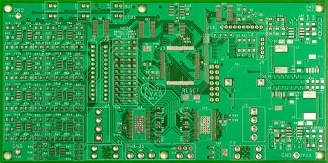
Solder mask layers are the protective layers of a PCB. They are made of a thin layer of polymer that is applied over the copper layers to protect them from oxidation and contamination. Solder mask layers also provide insulation between adjacent copper traces and pads.
Types of Solder Mask Colors
Solder mask layers are available in different colors, each with different properties and applications. The most common types of solder mask colors include:
| Color | Description | Applications |
|---|---|---|
| Green | Most common color | General-purpose PCBs |
| Red | High-contrast color | Prototyping and debugging |
| Blue | High-contrast color | Prototyping and debugging |
| Black | Helps with heat dissipation | High-power applications |
| White | Reflects light | LED applications |
4. Silkscreen Layers
Silkscreen layers are the labeling layers of a PCB. They are used to print text, logos, and other markings on the surface of the PCB. Silkscreen layers are typically made of a thin layer of epoxy ink that is applied over the solder mask layer.
Types of Silkscreen Colors
Silkscreen layers are available in different colors, each with different properties and applications. The most common types of silkscreen colors include:
| Color | Description | Applications |
|---|---|---|
| White | Most common color | General-purpose PCBs |
| Black | High-contrast color | Prototyping and debugging |
| Yellow | High-visibility color | Warning labels and markings |
PCB Layer Stackup
The arrangement of the different types of PCB layers is known as the layer stackup. The layer stackup is an important consideration in PCB design, as it affects the electrical performance, mechanical strength, and manufacturing cost of the PCB.
Types of PCB Layer Stackups
There are several types of PCB layer stackups, each with different advantages and disadvantages. The most common types of PCB layer stackups include:
1. Single-Layer PCBs
Single-layer PCBs are the simplest and most basic type of PCB. They consist of a single copper layer on one side of the substrate material. Single-layer PCBs are typically used for simple, low-cost applications such as LED lighting and power supplies.
2. Double-Layer PCBs
Double-layer PCBs consist of two copper layers, one on each side of the substrate material. Double-layer PCBs are more complex than single-layer PCBs and allow for more efficient routing of electrical signals. They are commonly used in applications such as consumer electronics and industrial control systems.
3. Multi-Layer PCBs
Multi-layer PCBs consist of three or more copper layers, separated by insulating substrate layers. Multi-layer PCBs are the most complex and expensive type of PCB, but they offer the highest level of functionality and performance. They are commonly used in applications such as aerospace, defense, and high-speed communications.
Factors to Consider When Choosing a PCB Layer Stackup
When choosing a PCB layer stackup, there are several factors to consider, including:
-
Electrical Performance: The layer stackup should be designed to optimize signal integrity, reduce crosstalk, and minimize EMI.
-
Mechanical Strength: The layer stackup should provide adequate mechanical support and prevent warping or bending of the PCB.
-
Manufacturing Cost: The layer stackup should be designed to minimize manufacturing costs while still meeting the required specifications.
-
Application Requirements: The layer stackup should be chosen based on the specific requirements of the application, such as operating temperature, shock and vibration resistance, and environmental conditions.

PCB Layer Design Considerations
When designing a PCB, there are several important considerations to keep in mind to ensure optimal performance and reliability. Some of the key design considerations include:
1. Signal Integrity
Signal integrity refers to the quality of the electrical signals transmitted through the PCB. To ensure good signal integrity, designers must carefully consider factors such as trace width, spacing, and impedance matching. They must also minimize crosstalk and EMI by using techniques such as ground planes, shielding, and filtering.
2. Power Distribution
Power distribution refers to the delivery of power to the components on the PCB. To ensure reliable power distribution, designers must carefully consider factors such as voltage drop, current capacity, and thermal management. They must also use techniques such as power planes, decoupling capacitors, and voltage regulators to maintain stable power supply voltages.
3. Thermal Management
Thermal management refers to the dissipation of heat generated by the components on the PCB. To ensure reliable operation and prevent component failure, designers must carefully consider factors such as component placement, airflow, and thermal vias. They must also use techniques such as heatsinks, fans, and thermal interface materials to remove heat from the PCB.
4. Manufacturing Considerations
Manufacturing considerations refer to the factors that affect the manufacturability and cost of the PCB. To ensure efficient and cost-effective manufacturing, designers must carefully consider factors such as minimum trace width and spacing, hole size and spacing, and soldermask and silkscreen design. They must also follow industry standards and guidelines for PCB design and manufacturing.
PCB Layer Manufacturing Process
The manufacturing process for PCBs involves several steps, each of which is critical to ensuring the quality and reliability of the final product. The basic steps in the PCB manufacturing process include:
1. Substrate Preparation
The first step in the PCB manufacturing process is to prepare the substrate material. This involves cutting the substrate to the required size and shape, drilling holes for vias and component leads, and cleaning the surface to remove any contaminants.
2. Copper Deposition
The next step is to deposit a thin layer of copper onto the substrate material. This is typically done using a process called electroless plating, which involves immersing the substrate in a chemical bath that contains copper ions. The copper ions are attracted to the surface of the substrate and form a thin, even layer of copper.
3. Patterning
Once the copper layer has been deposited, the next step is to create the desired circuit pattern on the surface of the PCB. This is typically done using a process called photolithography, which involves applying a light-sensitive resist material to the surface of the copper layer and exposing it to light through a patterned mask. The exposed areas of the resist are then removed, leaving behind a pattern of exposed copper.
4. Etching
The exposed copper is then removed using a chemical etching process, leaving behind the desired circuit pattern on the surface of the PCB.
5. Lamination
If the PCB has multiple layers, the next step is to laminate the layers together using heat and pressure. This involves stacking the layers on top of each other with insulating material between them and applying heat and pressure to bond them together.
6. Drilling
After lamination, holes are drilled through the PCB to allow for the insertion of component leads and vias. The holes are typically drilled using a CNC machine, which can precisely control the location and size of each hole.
7. Plating
The holes are then plated with copper to provide electrical connections between layers. This is typically done using a process called electroplating, which involves immersing the PCB in a chemical bath that contains copper ions and applying an electrical current to attract the ions to the surface of the holes.
8. Solder Mask and Silkscreen
The final steps in the PCB manufacturing process are to apply the solder mask and silkscreen layers. The solder mask is applied to the surface of the PCB to protect the copper traces from oxidation and to prevent solder from bridging between adjacent pads. The silkscreen layer is then applied to the surface of the solder mask to provide labeling and marking for components and other features.
Frequently Asked Questions (FAQ)
1. What is the difference between a single-layer and a multi-layer PCB?
A single-layer PCB has only one layer of copper, while a multi-layer PCB has two or more layers of copper separated by insulating layers. Multi-layer PCBs offer higher density and better signal integrity than single-layer PCBs, but they are also more complex and expensive to manufacture.
2. How many layers can a PCB have?
The number of layers in a PCB can vary depending on the complexity of the circuit and the requirements of the application. Most PCBs have between 2 and 8 layers, but some high-density PCBs can have up to 50 layers or more.
3. What is the purpose of the solder mask layer on a PCB?
The solder mask layer is a protective coating that is applied to the surface of the PCB to protect the copper traces from oxidation and to prevent solder from bridging between adjacent pads. It also provides insulation between the copper traces and helps to prevent short circuits.
4. What is the difference between a power plane and a ground plane in a PCB?
A power plane is a copper layer that is used to distribute power to the components on the PCB, while a ground plane is a copper layer that is used to provide a low-impedance return path for the current. Power planes and ground planes are typically used in multi-layer PCBs to provide better power distribution and signal integrity.
5. What are some common materials used for PCB substrates?
Some common materials used for PCB substrates include FR-4, which is a glass-reinforced epoxy laminate, and polyimide, which is a high-temperature plastic. Other materials such as ceramic and metal-core substrates are also used in specialized applications.
Conclusion
PCB layers are a critical component of modern electronic devices, providing the necessary electrical connections and insulation to ensure reliable and efficient operation. Understanding the different types of PCB layers and their functions is essential for anyone involved in the design or manufacturing of electronic products.
By considering factors such as signal integrity, power distribution, thermal management, and manufacturing considerations, designers can create PCBs that meet the specific requirements of their applications while minimizing costs and maximizing reliability.
As technology continues to advance and electronic devices become more complex, the importance of PCB layers will only continue to grow. By staying up-to-date with the latest developments in PCB design and manufacturing, engineers and manufacturers can ensure that their products remain at the forefront of innovation and performance.
Leave a Reply