What is PCB CAM?
PCB CAM, which stands for Printed Circuit Board Computer-Aided Manufacturing, is a crucial process in the production of printed circuit boards (PCBs). It involves using specialized software to convert the electronic design files, such as Gerber files, into machine-readable instructions that can be used by the manufacturing equipment to fabricate the PCB.
The PCB CAM process is an essential step in the PCB manufacturing workflow, bridging the gap between the design phase and the actual production of the board. It ensures that the design intent is accurately translated into the physical product, taking into account the specific requirements and constraints of the manufacturing process.
Key Steps in the PCB CAM Process
-
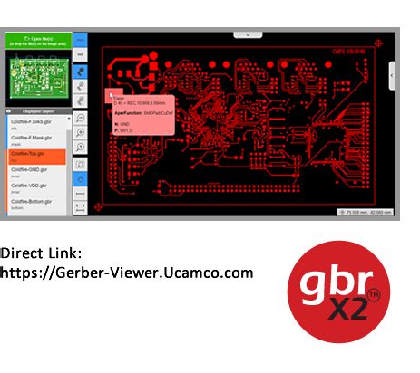
Data Input: The first step in the PCB CAM process is to import the electronic design files, typically in the form of Gerber files, into the CAM software. These files contain the necessary information about the PCB layout, including the copper layers, solder mask, silkscreen, and drill data.
-
Data Verification: Once the design files are imported, the CAM software performs a series of checks to verify the integrity and completeness of the data. This includes checking for missing or incorrect layers, aperture lists, and drill files. Any errors or discrepancies are identified and corrected at this stage.
-
Panelization: In order to optimize the manufacturing process and reduce costs, multiple PCBs are often fabricated together on a single panel. The CAM software is used to arrange the individual PCB designs into an optimal panel layout, taking into account factors such as board size, spacing, and tooling holes.
-
Toolpath Generation: Based on the verified design data and the panel layout, the CAM software generates the necessary toolpaths for the manufacturing equipment. This includes the paths for drilling, milling, and routing operations, as well as the data for solder mask and silkscreen application.
-
Output Generation: Finally, the CAM software generates the machine-readable output files that will be used by the manufacturing equipment. These files, often in the form of Gerber or NC drill files, contain the detailed instructions for fabricating the PCB, including the specific tools, speeds, and feeds to be used.
The Role of PCB CAM in Prototyping
PCB Prototyping is an essential step in the product development process, allowing designers and engineers to test and validate their designs before committing to full-scale production. The PCB CAM process plays a critical role in the prototyping phase, ensuring that the prototype boards accurately reflect the design intent and meet the necessary performance and reliability requirements.
Benefits of PCB CAM in Prototyping
-
Improved Accuracy: The PCB CAM process helps to ensure that the prototype boards are fabricated accurately, with minimal errors or defects. By using specialized software to convert the design files into machine-readable instructions, the risk of human error is greatly reduced, resulting in higher quality prototypes.
-
Faster Turnaround Times: The automated nature of the PCB CAM process allows for faster generation of the manufacturing data, reducing the overall time required to produce the prototype boards. This is particularly important in the prototyping phase, where quick iterations and design changes are often necessary.
-
Cost Reduction: By optimizing the panel layout and toolpaths, the PCB CAM process helps to minimize material waste and reduce the overall manufacturing costs. This is especially beneficial in the prototyping phase, where cost-effectiveness is crucial to allow for multiple design iterations.
-
Design Validation: The PCB CAM process helps to validate the design files before the prototype boards are manufactured. By performing checks for data integrity and completeness, any issues or errors can be identified and corrected early in the process, reducing the risk of costly mistakes or delays.
Considerations for PCB CAM in Prototyping
-
Design for Manufacturability (DFM): When designing PCBs for prototyping, it is important to consider the manufacturability of the design. The PCB CAM process can help identify potential manufacturing challenges or constraints, such as minimum feature sizes, spacing requirements, or drill limitations. By incorporating DFM principles into the design, the prototyping process can be streamlined and the overall manufacturability of the product can be improved.
-
Material Selection: The choice of materials for the Prototype PCBs can have a significant impact on the performance and reliability of the final product. The PCB CAM process can help ensure that the selected materials are compatible with the manufacturing process and meet the necessary requirements for the intended application. This includes considerations such as the substrate material, copper weight, and surface finish.
-
Testing and Validation: Once the prototype boards have been fabricated, it is important to perform thorough testing and validation to ensure that they meet the design requirements and perform as expected. The PCB CAM process can help facilitate this by providing accurate and reliable manufacturing data, ensuring that the prototype boards are consistent with the original design intent.

Best Practices for PCB CAM in Prototyping
To optimize the PCB CAM process for prototyping, consider the following best practices:
-
Use a Reliable CAM Software: Choose a reputable and reliable CAM software that is compatible with your design tools and manufacturing equipment. Look for software with advanced features such as design rule checking (DRC), panelization, and automatic toolpath generation.
-
Ensure Data Integrity: Double-check the design files for accuracy and completeness before submitting them for CAM processing. Ensure that all necessary layers, aperture lists, and drill files are included and properly formatted.
-
Communicate with the Manufacturer: Work closely with your PCB manufacturer throughout the prototyping process. Provide clear and detailed instructions, including any specific requirements or constraints. Be open to feedback and suggestions from the manufacturer regarding design modifications or process improvements.
-
Plan for Iterations: Anticipate the need for multiple design iterations during the prototyping phase. Structure your PCB CAM process to accommodate quick turnarounds and design changes, allowing for efficient and cost-effective revisions.
-
Document the Process: Maintain detailed documentation of the PCB CAM process, including the design files, manufacturing data, and any changes or modifications made along the way. This documentation can be invaluable for future reference, troubleshooting, or process improvement.

Frequently Asked Questions (FAQ)
- What is the difference between PCB CAM and PCB CAD?
-
PCB CAD (Computer-Aided Design) refers to the process of designing the PCB layout using specialized software, while PCB CAM (Computer-Aided Manufacturing) involves converting the design files into machine-readable instructions for manufacturing.
-
Can PCB CAM be used for both prototype and production PCBs?
-
Yes, PCB CAM is used for both prototype and production PCBs. However, the specific requirements and considerations may differ between the two, with prototyping often requiring faster turnaround times and more frequent design iterations.
-
What are the most common file formats used in PCB CAM?
-
The most common file formats used in PCB CAM include Gerber files (RS-274X) for the PCB Layers, NC drill files for the drilling data, and ODB++ (Open Database) for the complete PCB design data.
-
How does PCB CAM help with Design for Manufacturability (DFM)?
-
PCB CAM software often includes DFM analysis tools that can identify potential manufacturing issues or constraints early in the design process. By flagging these issues and providing suggestions for improvement, PCB CAM helps ensure that the design is optimized for manufacturability.
-
What are the benefits of using a reputable PCB CAM service provider for prototyping?
- Using a reputable PCB CAM service provider for prototyping can offer several benefits, including access to advanced software and equipment, experienced technicians, and streamlined processes. This can result in faster turnaround times, higher quality prototypes, and more cost-effective solutions.
| Aspect | PCB CAD | PCB CAM |
|---|---|---|
| Purpose | Design the PCB layout | Convert design files into manufacturing instructions |
| Software | PCB design software (e.g., Altium, KiCad, Eagle) | CAM software (e.g., CAM350, Genesis 2000, UCAMCO) |
| Key Tasks | Schematic capture, layout design, routing | Data verification, panelization, toolpath generation |
| File Formats | Schematic files, PCB layout files | Gerber files, NC drill files, ODB++ |
| Design Considerations | Component placement, signal integrity, EMI/EMC | Manufacturing constraints, DFM, material selection |
| Outcome | Complete PCB design ready for manufacturing | Machine-readable instructions for PCB fabrication |
In conclusion, the PCB CAM process is a critical step in the prototyping and production of printed circuit boards. By converting the electronic design files into machine-readable instructions, PCB CAM ensures that the design intent is accurately translated into the physical product, taking into account the specific requirements and constraints of the manufacturing process.
In the prototyping phase, PCB CAM offers several benefits, including improved accuracy, faster turnaround times, cost reduction, and design validation. By considering factors such as Design for Manufacturability (DFM), material selection, and testing and validation, the PCB CAM process can be optimized to streamline the prototyping process and improve the overall quality and reliability of the final product.
To achieve the best results, it is important to follow best practices for PCB CAM in prototyping, such as using reliable CAM software, ensuring data integrity, communicating with the manufacturer, planning for iterations, and documenting the process. By working with a reputable PCB CAM service provider and leveraging their expertise and resources, designers and engineers can effectively navigate the prototyping phase and bring their innovative ideas to life.


Leave a Reply