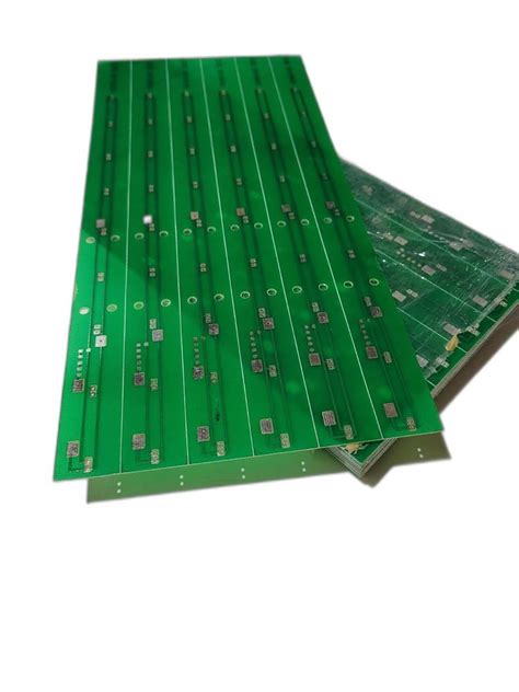
What is PCB Fabrication?
PCB fabrication is the process of creating a printed circuit board, which is used to mechanically support and electrically connect electronic components using conductive pathways, tracks, or signal traces etched from copper sheets laminated onto a non-conductive substrate.
The PCB Fabrication Process
The PCB fabrication process consists of several steps, each of which is critical to ensuring the quality and functionality of the final product. These steps include:
- Design and Layout
- Printing and Etching
- Drilling and Plating
- Solder Mask Application
- Silkscreen Printing
- Surface Finish Application
- Electrical Testing and Inspection
1. Design and Layout
The first step in PCB fabrication is the design and layout of the circuit board. This involves creating a schematic diagram of the circuit and then translating that schematic into a physical layout using PCB design software. The layout must take into account factors such as component placement, signal integrity, and manufacturability.
2. Printing and Etching
Once the layout is finalized, the next step is to print the circuit pattern onto the copper-clad board. This is typically done using a photoresist process, where a photosensitive material is applied to the board and then exposed to light through a photomask containing the circuit pattern. The exposed areas of the photoresist are then developed and removed, leaving behind the desired circuit pattern.
After the photoresist is developed, the board undergoes an etching process to remove the unwanted copper, leaving behind only the desired circuit traces.
3. Drilling and Plating
With the circuit pattern etched onto the board, the next step is to drill holes for through-hole components and vias (vertical interconnect access). These holes are then plated with a conductive material, typically copper, to ensure electrical conductivity between the layers of the board.
4. Solder Mask Application
A solder mask is a protective coating applied to the PCB to prevent short circuits and protect the copper traces from oxidation and other environmental factors. The solder mask is typically green in color but can be found in other colors as well.
5. Silkscreen Printing
Silkscreen printing is used to add text, logos, and other markings to the PCB. This is typically done using a white or yellow ink and helps with component placement and identification during assembly.
6. Surface Finish Application
The surface finish is a coating applied to the exposed copper on the PCB to protect it from oxidation and enhance solderability. There are several types of surface finishes available, including:
- HASL (Hot Air Solder Leveling)
- ENIG (Electroless Nickel Immersion Gold)
- OSP (Organic Solderability Preservative)
- Immersion Silver
- Immersion Tin
The choice of surface finish depends on factors such as the intended use of the PCB, the components being used, and the desired shelf life.
7. Electrical Testing and Inspection
The final step in the PCB fabrication process is electrical testing and inspection. This involves using specialized equipment to test the continuity and functionality of the board, as well as visually inspecting it for any defects or issues.
Types of PCBs
There are several types of PCBs, each with its own unique characteristics and applications. The most common types include:
- Single-sided PCBs
- Double-sided PCBs
- Multi-layer PCBs
- Flexible PCBs
- Rigid-Flex PCBs
| PCB Type | Layers | Applications |
|---|---|---|
| Single-sided | 1 | Simple, low-cost devices |
| Double-sided | 2 | More complex devices, better space utilization |
| Multi-layer | 3+ | High-density, complex devices |
| Flexible | 1-2 | Wearables, compact devices |
| Rigid-Flex | Varies | High-reliability, space-constrained devices |
PCB Materials
The choice of materials used in PCB fabrication is critical to the performance and reliability of the final product. The most common materials used include:
Substrates
- FR-4 (Flame Retardant 4)
- Rogers (High-frequency)
- Polyimide (High-temperature)
- Aluminum (Metal-core)
Copper
Copper is used for the conductive traces on the PCB. The thickness of the copper is typically measured in ounces per square foot (oz/ft²), with common thicknesses being 0.5 oz/ft², 1 oz/ft², and 2 oz/ft².
Solder Mask
The solder mask is typically made from a photoimageable polymer and is available in various colors, with green being the most common.
Silkscreen
The silkscreen ink is typically a white or yellow epoxy-based ink that is resistant to solvents and abrasion.

PCB Design Considerations
Designing a PCB involves more than just placing components and routing traces. There are several key considerations that must be taken into account to ensure the reliability and functionality of the final product.
Signal Integrity
Signal integrity refers to the quality of the electrical signals transmitted through the PCB. Factors that can affect signal integrity include:
- Trace length and routing
- Impedance matching
- Crosstalk
- Electromagnetic interference (EMI)
Thermal Management
Proper thermal management is essential to ensure the longevity and reliability of the PCB and its components. This involves considering factors such as:
- Component placement
- Copper thickness and density
- Thermal vias
- Heatsinks and cooling solutions
Manufacturing Constraints
PCB design must also take into account the constraints and limitations of the manufacturing process. This includes factors such as:
- Minimum trace width and spacing
- Hole sizes and spacing
- Clearance and creepage distances
- Soldermask and silkscreen tolerances

Advanced PCB Fabrication Techniques
In addition to the standard PCB fabrication process, there are several advanced techniques that can be used to create high-performance, specialized PCBs.
High-Density Interconnect (HDI)
HDI PCBs use smaller vias and traces to achieve higher component density and improved signal integrity. This involves techniques such as:
- Microvias
- Blind and buried vias
- Sequential lamination
Embedded Components
Embedded components are placed inside the PCB substrate, rather than on the surface. This can save space and improve signal integrity, but requires specialized manufacturing processes.
3D PCBs
3D PCBs are a relatively new technology that allows for the creation of three-dimensional circuit structures. This can enable new design possibilities and improved performance in certain applications.

PCB Testing and Inspection
Thorough testing and inspection are critical to ensuring the quality and reliability of PCBs. Some common testing and inspection methods include:
- Automated Optical Inspection (AOI)
- X-ray Inspection
- In-Circuit Testing (ICT)
- Flying Probe Testing
- Functional Testing
| Method | Purpose |
|---|---|
| AOI | Detect surface defects and component placement issues |
| X-ray | Inspect internal structures and solder joints |
| ICT | Test individual components and circuits |
| Flying Probe | Test electrical connectivity and component functionality |
| Functional Testing | Verify overall board functionality and performance |
Frequently Asked Questions (FAQ)
1. What is the difference between a PCB and a PCBA?
A PCB (Printed Circuit Board) is the bare board with copper traces, while a PCBA (Printed Circuit Board Assembly) is a PCB with components soldered onto it.
2. What is the typical turnaround time for PCB fabrication?
Turnaround time can vary depending on the complexity of the board and the manufacturer, but typically ranges from 1-2 weeks for standard orders and 3-5 days for expedited orders.
3. What is the minimum feature size for PCB traces and spacing?
The minimum feature size depends on the PCB fabrication capabilities of the manufacturer but typically ranges from 3-4 mils (thousandths of an inch) for standard PCBs and down to 1-2 mils for advanced HDI PCBs.
4. Can I combine different surface finishes on the same PCB?
Yes, it is possible to use different surface finishes on different areas of the PCB, such as ENIG for connectors and OSP for other components. However, this may increase the cost and complexity of the fabrication process.
5. How do I choose the right material for my PCB substrate?
The choice of substrate material depends on factors such as the intended application, operating environment, frequency, and cost. FR-4 is the most common material for general-purpose PCBs, while high-frequency materials like Rogers or high-temperature materials like polyimide may be needed for specialized applications.
Conclusion
PCB fabrication is a complex process that involves a wide range of materials, techniques, and considerations. By understanding the basics of PCB fabrication and the key factors that influence the performance and reliability of PCBs, engineers and designers can create high-quality, robust electronic devices that meet the needs of their intended applications.
As technology continues to advance, new materials and fabrication techniques will undoubtedly emerge, enabling even greater possibilities for PCB design and performance. By staying up-to-date with the latest developments and best practices in PCB fabrication, engineers and manufacturers can stay ahead of the curve and create innovative, cutting-edge electronic products.


Leave a Reply