What is PCB Manufacturing?
PCB manufacturing is the process of fabricating printed circuit boards (PCBs) that electrically connect and mechanically support electronic components using conductive pathways, tracks, or signal traces etched from copper sheets laminated onto a non-conductive substrate. It is a complex multi-step process that starts with PCB design and ends with final inspection and testing before the PCB is ready for assembly into an electronic device.
The global PCB market size was valued at USD 61.5 billion in 2020 and is expected to expand at a compound annual growth rate (CAGR) of 4.3% from 2021 to 2028. The increasing demand for PCBs in consumer electronics, automotive, healthcare, aerospace and defense, and other industries is driving the growth of the PCB manufacturing market.
PCB Manufacturing Process Overview
The PCB manufacturing process involves several steps, each of which requires precision, accuracy, and adherence to strict quality control standards. The following table provides an overview of the main steps involved in PCB manufacturing:
| Step | Description |
|---|---|
| PCB Design | Creating the schematic diagram and layout of the PCB using CAD software |
| Printing Film | Printing the PCB design onto a clear film or mask |
| Copper Clad Laminate | Selecting the appropriate copper clad laminate based on the PCB specifications |
| Drilling | Drilling holes into the PCB substrate for through-hole components and vias |
| Plating | Applying a thin layer of copper onto the drilled holes and traces |
| Etching | Removing unwanted copper from the PCB substrate to create the desired circuit pattern |
| Soldermask Application | Applying a layer of soldermask to protect the copper traces and prevent solder bridging |
| Silkscreen Printing | Printing text, symbols, and logos onto the PCB for identification and assembly purposes |
| Surface Finish | Applying a surface finish to the exposed copper to prevent oxidation and enhance solderability |
| Electrical Testing | Performing electrical tests to ensure the PCB functions as intended |
| Final Inspection | Visually inspecting the PCB for any defects or imperfections |
PCB Design
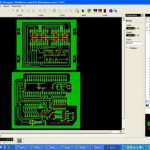
The PCB manufacturing process begins with PCB design. The PCB design is created using computer-aided design (CAD) software, such as Altium, Eagle, or KiCad. The design includes the schematic diagram, which shows the electrical connections between components, and the PCB layout, which shows the physical placement of components and tracks on the board.
The PCB designer must consider several factors when creating the design, such as:
- The number of layers required
- The size and shape of the PCB
- The placement of components and connectors
- The width and spacing of tracks
- The electrical characteristics of the design (e.g., impedance, crosstalk)
Once the PCB design is complete, it is sent to the PCB manufacturer for fabrication.
Printing Film
The next step in the PCB manufacturing process is printing the PCB design onto a clear film or photo mask. This film is used to transfer the circuit pattern onto the copper clad laminate during the etching process.
The PCB design files are sent to a photoplotter, which uses a laser or LED light source to expose the design onto the film. The film is then developed, similar to traditional photography, to create a high-contrast image of the circuit pattern.
Copper Clad Laminate
The foundation of the PCB is the copper clad laminate, which consists of a thin layer of copper foil bonded to a non-conductive substrate material, such as FR-4 glass-reinforced epoxy. The thickness and type of copper clad laminate used depends on the specific requirements of the PCB, such as the number of layers, the required electrical properties, and the intended application.
The copper clad laminate is cut to the desired size and shape of the PCB using a CNC machine or a hydraulic shear. The copper surface is then cleaned and prepared for the subsequent manufacturing steps.
Drilling
Once the copper clad laminate is prepared, the next step is drilling holes into the board for through-hole components and vias. Vias are small holes that allow electrical connections between different layers of the PCB.
The drilling process is performed using a CNC drilling machine, which uses high-speed drill bits to create precise holes in the PCB substrate. The drill bit size and placement are determined by the PCB design files.
After drilling, the holes are cleaned and deburred to remove any rough edges or debris that could interfere with the subsequent plating process.
Plating
The next step in the PCB manufacturing process is plating. Plating involves applying a thin layer of copper onto the drilled holes and traces to create a conductive pathway for electrical current.
There are two main types of plating used in PCB manufacturing:
-
Electroless plating: This process involves immersing the PCB in a chemical solution that deposits a thin layer of copper onto the surface of the board and inside the drilled holes. Electroless plating is typically used for high-volume production and provides good coverage and adhesion.
-
Electrolytic plating: This process involves applying an electrical current to the PCB while it is immersed in a copper sulfate solution. The electrical current attracts the copper ions to the surface of the board and inside the drilled holes, creating a thicker and more conductive layer of copper. Electrolytic plating is typically used for high-performance applications that require a thicker layer of copper.
After plating, the PCB is rinsed and dried to remove any excess solution or debris.
Etching
The etching process is used to remove unwanted copper from the PCB substrate, leaving only the desired circuit pattern. There are two main methods of etching used in PCB manufacturing:
-
Wet etching: This process involves immersing the PCB in a chemical solution, such as ferric chloride or ammonium persulfate, which dissolves the unwanted copper. The PCB is then rinsed and dried to remove any remaining solution.
-
Dry etching: This process involves using a plasma or laser to remove the unwanted copper from the PCB substrate. Dry etching is typically used for high-precision applications that require fine feature sizes and tight tolerances.
The choice of etching method depends on the specific requirements of the PCB, such as the required feature size, the type of copper clad laminate used, and the production volume.
Soldermask Application
After etching, a layer of soldermask is applied to the PCB to protect the copper traces and prevent solder bridging during the assembly process. Soldermask is a thin, heat-resistant polymer coating that is applied to the PCB using a silkscreen printing process.
The soldermask is typically green in color, but other colors such as red, blue, or black are also available. The choice of soldermask color depends on the intended application and the aesthetic requirements of the PCB.
After the soldermask is applied, the PCB is exposed to ultraviolet (UV) light to cure and harden the coating. The PCB is then baked in an oven to fully cure the soldermask and improve its adhesion to the board.
Silkscreen Printing
Silkscreen printing is used to print text, symbols, and logos onto the PCB for identification and assembly purposes. The silkscreen design is created using CAD software and then transferred onto a fine mesh screen.
The PCB is placed underneath the screen, and ink is forced through the mesh onto the surface of the board using a squeegee. The ink is then cured using UV light or heat to create a permanent print.
Silkscreen printing is typically used for applying part numbers, company logos, and other identifying marks to the PCB. It is also used for creating assembly instructions, such as component placement indicators and polarity marks.
Surface Finish
The final step in the PCB manufacturing process is applying a surface finish to the exposed copper on the board. The surface finish serves several purposes, including:
- Protecting the copper from oxidation and corrosion
- Enhancing the solderability of the copper during the assembly process
- Improving the electrical conductivity and signal integrity of the PCB
There are several types of surface finishes used in PCB manufacturing, including:
- Hot Air Solder Leveling (HASL): A thin layer of solder is applied to the copper surfaces of the PCB using a hot air knife. HASL is a low-cost and widely used surface finish, but it can lead to uneven surfaces and reduced flatness.
- Electroless Nickel Immersion Gold (ENIG): A layer of nickel is deposited onto the copper surfaces, followed by a thin layer of gold. ENIG provides excellent solderability and corrosion resistance, but it is more expensive than other surface finishes.
- Immersion Silver (IAg): A thin layer of silver is chemically deposited onto the copper surfaces of the PCB. IAg provides good solderability and is a lower-cost alternative to ENIG.
- Immersion Tin (ISn): A thin layer of tin is chemically deposited onto the copper surfaces of the PCB. ISn provides good solderability and is a lower-cost alternative to ENIG and IAg.
- Organic Solderability Preservative (OSP): A thin, organic coating is applied to the copper surfaces of the PCB to prevent oxidation and enhance solderability. OSP is a low-cost and environmentally friendly surface finish, but it has a limited shelf life and may require special handling during assembly.
The choice of surface finish depends on the specific requirements of the PCB, such as the intended application, the assembly process, and the budget.
Electrical Testing
After the surface finish is applied, the PCB undergoes electrical testing to ensure that it functions as intended. There are several types of electrical tests performed on PCBs, including:
- Continuity Test: This test checks for any open or short circuits in the PCB by measuring the resistance between various points on the board.
- Insulation Resistance Test: This test measures the resistance between different conductors on the PCB to ensure that there is no leakage current or insulation breakdown.
- High-Potential Test: This test applies a high voltage to the PCB to check for any insulation breakdowns or leakage currents.
- Impedance Test: This test measures the impedance of the PCB traces to ensure that they meet the required specifications for signal integrity and high-speed performance.
Automated test equipment (ATE) is often used to perform these electrical tests on PCBs. The ATE uses a bed of nails fixture or a Flying Probe to make contact with the test points on the PCB and perform the necessary measurements.
Final Inspection
The final step in the PCB manufacturing process is visual inspection. The PCB is inspected under magnification to check for any defects or imperfections, such as:
- Scratches or nicks in the copper traces
- Voids or pinholes in the soldermask or silkscreen
- Incomplete or excess plating in the holes and vias
- Contamination or foreign objects on the surface of the board
Automated optical inspection (AOI) equipment is often used to perform the visual inspection of PCBs. The AOI Equipment uses high-resolution cameras and image processing software to detect and classify defects on the PCB surface.
Once the PCB passes the final inspection, it is packaged and shipped to the customer for assembly and integration into the final product.
PCB Manufacturing FAQs
-
What is the typical turnaround time for PCB manufacturing?
The typical turnaround time for PCB manufacturing depends on the complexity and quantity of the PCBs being produced. For simple, low-volume orders, the turnaround time can be as short as 24-48 hours. For more complex, high-volume orders, the turnaround time can be several weeks or longer. -
What is the minimum order quantity for PCB manufacturing?
The minimum order quantity (MOQ) for PCB manufacturing varies depending on the manufacturer and the complexity of the PCBs being produced. Some manufacturers offer low MOQs of 5-10 pieces for prototyping and small-volume production, while others require higher MOQs of 100 pieces or more for larger production runs. -
What is the typical cost per unit for PCB manufacturing?
The cost per unit for PCB manufacturing depends on several factors, including the complexity of the design, the quantity being produced, and the materials and surface finishes used. In general, the cost per unit decreases as the quantity increases, due to economies of scale. For small-volume orders, the cost per unit can range from a few dollars to several hundred dollars, depending on the complexity of the PCB. For large-volume orders, the cost per unit can be less than a dollar. -
What are the environmental considerations for PCB manufacturing?
PCB manufacturing can have significant environmental impacts, due to the use of hazardous chemicals and materials in the production process. Some of the key environmental considerations for PCB manufacturing include: - The use of lead-free solder and other materials to reduce the environmental impact of e-waste
- The proper handling and disposal of hazardous chemicals and waste products generated during the manufacturing process
- The use of renewable energy sources and energy-efficient equipment to reduce the carbon footprint of PCB manufacturing
-
The implementation of environmental management systems and certifications, such as ISO 14001, to ensure compliance with environmental regulations and best practices.
-
What are the quality control standards for PCB manufacturing?
PCB manufacturing is subject to strict quality control standards to ensure the reliability and performance of the final product. Some of the key quality control standards for PCB manufacturing include: - IPC (Association Connecting Electronics Industries) standards, which provide guidelines for the design, fabrication, assembly, and testing of PCBs
- ISO 9001 certification, which ensures that the manufacturer has a quality management system in place to consistently meet customer and regulatory requirements
- UL (Underwriters Laboratories) certification, which ensures that the PCBs meet safety and performance standards for the intended application
- Mil-Spec (Military Specification) standards, which provide guidelines for the design and manufacturing of PCBs for military and aerospace applications.
In conclusion, PCB manufacturing is a complex and multi-step process that requires precision, accuracy, and adherence to strict quality control standards. From PCB design to final inspection, each step in the manufacturing process plays a critical role in ensuring the reliability and performance of the final product.
As the demand for PCBs continues to grow across various industries, PCB Manufacturers are investing in advanced technologies and processes to improve efficiency, reduce costs, and meet the evolving needs of their customers. At the same time, there is a growing emphasis on environmental sustainability and social responsibility in PCB manufacturing, as companies seek to minimize their environmental footprint and ensure fair labor practices throughout the supply chain.
By understanding the intricacies of PCB manufacturing and the key considerations for quality, cost, and environmental impact, designers, engineers, and procurement professionals can make informed decisions when sourcing PCBs for their projects. Whether for prototyping or high-volume production, partnering with a reputable and experienced PCB manufacturer is essential to ensuring the success and longevity of the final product.

Leave a Reply