What is Photolithography?
Photolithography, also known as optical lithography or UV lithography, is a process used in microfabrication to pattern parts of a thin film or the bulk of a substrate. It uses light to transfer a geometric pattern from a photomask to a photosensitive chemical photoresist on the substrate. A series of chemical treatments then either engraves the exposure pattern into the material or enables deposition of a new material in the desired pattern upon the material underneath the photoresist.
Photolithography is widely used in the fabrication of semiconductors, microelectromechanical systems (MEMS), DNA microarrays, and other microdevices. It is a crucial step in the manufacturing process of integrated circuits (ICs) such as computer processors and memory chips.
Key Components of Photolithography
The key components involved in the photolithography process are:
-
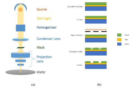
Substrate: The base material on which the photoresist is applied and the desired pattern is to be formed. Common substrates include silicon wafers, glass plates, and plastic films.
-
Photoresist: A light-sensitive material that undergoes a chemical change when exposed to light. There are two types of photoresists:
- Positive photoresist: The exposed areas become more soluble in the developer solution.
-
Negative photoresist: The exposed areas become less soluble in the developer solution.
-
Photomask: A transparent plate with opaque patterns that define the desired layout of the device. The photomask is placed between the light source and the photoresist-coated substrate during exposure.
-
Light source: A source of light with a specific wavelength that is used to expose the photoresist. Common light sources include mercury lamps, excimer lasers, and LED arrays.
-
Optical system: A set of lenses, mirrors, and filters that focus and shape the light beam onto the photoresist-coated substrate.
Photolithography Process Steps
The photolithography process involves several steps that are repeated for each layer of the device being fabricated. The main steps are:
1. Substrate Preparation
The substrate is cleaned to remove any contaminants or particles that could affect the quality of the final pattern. The cleaning process may involve chemical treatments, such as piranha solution or RCA clean, followed by a dehydration bake to remove moisture from the surface.
2. Photoresist Application
The photoresist is applied to the substrate using a spin coating technique. The substrate is placed on a spinner, and a small amount of photoresist is dispensed onto the center of the substrate. The spinner is then rotated at high speed (typically 1000-6000 rpm) to spread the photoresist evenly across the surface. The thickness of the photoresist layer is controlled by the spin speed and duration.
After spin coating, the photoresist-coated substrate is subjected to a soft bake (also known as a pre-bake) to remove any remaining solvent and to improve adhesion between the photoresist and the substrate.
3. Exposure
The photoresist-coated substrate is aligned with the photomask using an alignment system. The photomask is placed in close proximity to the substrate, and the assembly is exposed to light. The light passes through the transparent areas of the photomask and interacts with the photoresist, causing a chemical change in the exposed regions.
The exposure dose (the amount of light energy per unit area) and time are carefully controlled to ensure the desired pattern is formed in the photoresist.
4. Development
After exposure, the substrate is subjected to a post-exposure bake (PEB) to complete the chemical reaction initiated during exposure. The PEB helps to improve the contrast and resolution of the developed pattern.
The substrate is then immersed in a developer solution, which selectively dissolves either the exposed (for positive photoresist) or unexposed (for negative photoresist) areas of the photoresist. The development time is critical and must be carefully controlled to achieve the desired pattern dimensions.
5. Pattern Transfer
Once the photoresist pattern is developed, it can be used as a mask for subsequent processing steps, such as etching, ion implantation, or deposition. These processes transfer the photoresist pattern onto the underlying substrate or layers.
-
Etching: The exposed areas of the substrate are selectively removed using chemical or physical Etching Processes, such as wet etching (using liquid etchants) or dry etching (using plasma or reactive ion etching).
-
Ion implantation: Ions are accelerated and implanted into the exposed areas of the substrate to modify its electrical properties.
-
Deposition: Materials, such as metals or dielectrics, are deposited onto the exposed areas of the substrate using techniques like evaporation, sputtering, or chemical vapor deposition (CVD).
6. Photoresist Removal
After the pattern transfer step, the remaining photoresist is removed from the substrate using a stripping process. This can involve wet stripping (using solvents) or dry stripping (using plasma or reactive ion etching). The substrate is then cleaned to prepare it for the next layer of processing.

Resolution and Limitations
The resolution of photolithography is limited by the wavelength of the light source used for exposure. The minimum feature size that can be resolved is given by the Rayleigh criterion:
Resolution = k₁ × λ / NA
Where:
– k₁ is a process-dependent factor (typically 0.4-0.8)
– λ is the wavelength of the light source
– NA is the numerical aperture of the optical system
To achieve smaller feature sizes, advanced photolithography techniques have been developed, such as:
- Deep ultraviolet (DUV) lithography: Uses light sources with shorter wavelengths (248 nm or 193 nm) to improve resolution.
- Immersion lithography: Introduces a high-refractive-index fluid between the lens and the wafer to increase the effective NA and improve resolution.
- Multiple patterning: Involves splitting a single layer pattern into multiple exposures to overcome the resolution limit of a single exposure.
Despite these advancements, photolithography faces several challenges as feature sizes continue to shrink:
- Diffraction effects: As feature sizes approach the wavelength of the light source, diffraction effects become more pronounced, limiting the achievable resolution.
- Overlay accuracy: Aligning multiple layers with nanometer-scale precision becomes increasingly difficult as feature sizes decrease.
- Process variability: Maintaining tight control over process parameters, such as exposure dose, focus, and development time, becomes more challenging at smaller scales.

Applications of Photolithography
Photolithography has a wide range of applications in various fields, including:
Semiconductor Industry
Photolithography is the primary patterning technique used in the fabrication of integrated circuits, such as:
- Microprocessors
- Memory chips (DRAM, SRAM, Flash)
- Application-specific integrated circuits (ASICs)
- Field-programmable gate arrays (FPGAs)
Microelectromechanical Systems (MEMS)
Photolithography is used to create the complex 3D structures found in MEMS devices, such as:
- Accelerometers
- Gyroscopes
- Pressure sensors
- Micromirrors
Flat Panel Displays
Photolithography is used to pattern the thin-film transistor (TFT) arrays and color filters in flat panel displays, such as:
- Liquid crystal displays (LCDs)
- Organic light-emitting diode (OLED) displays
Biomedical Devices
Photolithography is used to fabricate microfluidic devices, biosensors, and other biomedical devices, such as:
- Lab-on-a-chip systems
- DNA microarrays
- Implantable sensors and drug delivery devices

Future of Photolithography
As the demand for smaller, faster, and more efficient electronic devices continues to grow, photolithography will need to evolve to meet these challenges. Some of the key areas of research and development in photolithography include:
Extreme Ultraviolet (EUV) Lithography
EUV lithography uses light with a wavelength of 13.5 nm to achieve even higher resolution than DUV lithography. However, EUV lithography faces several technical challenges, such as the development of high-power EUV light sources and the fabrication of defect-free EUV masks.
Directed Self-Assembly (DSA)
DSA is a technique that uses block copolymers to create nanoscale patterns through the self-assembly of polymer domains. DSA can potentially enable the fabrication of features smaller than those achievable with conventional photolithography.
Nanoimprint Lithography (NIL)
NIL is a mechanical patterning technique that uses a mold to transfer patterns onto a substrate. NIL has the potential to achieve high-resolution patterning at a lower cost than conventional photolithography.
As these and other technologies mature, photolithography will continue to play a critical role in the fabrication of advanced electronic devices and systems.
Frequently Asked Questions (FAQ)
- What is the difference between positive and negative photoresist?
-
Positive photoresist becomes more soluble in the developer solution when exposed to light, while negative photoresist becomes less soluble when exposed. As a result, the exposed areas of positive photoresist are removed during development, while the exposed areas of negative photoresist remain after development.
-
What factors affect the resolution of photolithography?
-
The resolution of photolithography is primarily determined by the wavelength of the light source, the numerical aperture of the optical system, and process-dependent factors such as the photoresist and development conditions. Smaller wavelengths and higher numerical apertures generally lead to higher resolution.
-
What is the purpose of the post-exposure bake (PEB) in photolithography?
-
The post-exposure bake is performed after the exposure step to complete the chemical reaction initiated during exposure. The PEB helps to improve the contrast and resolution of the developed photoresist pattern by reducing the effects of standing waves and diffusion.
-
What is the difference between wet and dry etching?
-
Wet etching uses liquid chemical etchants to selectively remove material from the substrate, while dry etching uses plasma or reactive ion etching to remove material. Wet etching is generally more selective but less anisotropic than dry etching, which can achieve highly directional etching profiles.
-
What are some of the challenges faced by photolithography as feature sizes continue to shrink?
- As feature sizes approach the wavelength of the light source, diffraction effects become more pronounced, limiting the achievable resolution. Maintaining overlay accuracy and tight control over process parameters also becomes increasingly difficult at smaller scales. Additionally, the development of new materials and processes is required to enable the fabrication of sub-10 nm features.
Conclusion
Photolithography is a critical technology that has enabled the rapid advancement of the semiconductor industry and related fields over the past several decades. By using light to transfer patterns onto a substrate, photolithography allows for the fabrication of complex, high-resolution structures at the micro- and nanoscale.
As the demand for smaller, faster, and more efficient electronic devices continues to grow, photolithography will need to evolve to meet these challenges. Researchers and engineers are actively developing new technologies, such as EUV lithography, directed self-assembly, and nanoimprint lithography, to push the boundaries of what is possible with photolithography.
Despite the challenges ahead, photolithography will undoubtedly remain a key enabling technology for the foreseeable future, driving innovation and progress in fields ranging from computing and communications to healthcare and renewable energy.


Leave a Reply