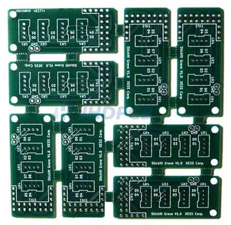
What is PCB Panelization?
PCB panelization is the process of combining multiple printed circuit board (PCB) designs onto a single panel for manufacturing. This technique is used to increase production efficiency and reduce costs by allowing multiple PCBs to be fabricated simultaneously. Panelization is particularly useful when dealing with small or oddly shaped PCBs, such as round-shaped boards, as it helps optimize the use of materials and streamline the assembly process.
Benefits of PCB Panelization
- Cost reduction
- Increased production efficiency
- Improved handling and assembly
- Optimized material usage
Challenges in Panelizing Round-Shaped PCBs
Round-shaped PCBs present unique challenges when it comes to panelization. Unlike rectangular boards, round PCBs have curved edges that can make it difficult to arrange them efficiently on a panel. Additionally, the panelization process must take into account the specific requirements of the round PCB design, such as the placement of components and the need for proper spacing between individual boards.
Common Issues in Round PCB Panelization
- Inefficient panel utilization
- Difficulty in maintaining proper spacing
- Increased risk of damage during depaneling
- Limitations in component placement

Techniques for Panelizing Round PCBs
To overcome the challenges associated with panelizing round PCBs, several techniques can be employed. These methods aim to maximize panel utilization, ensure proper spacing, and facilitate smooth depaneling.
1. Tessellation
Tessellation involves arranging the round PCBs in a pattern that minimizes the space between individual boards. By carefully positioning the PCBs, it is possible to create a tight-fitting arrangement that maximizes panel utilization. Common tessellation patterns for round PCBs include:
- Hexagonal packing
- Square packing
- Triangular packing
| Pattern | Description | Advantages | Disadvantages |
|---|---|---|---|
| Hexagonal | PCBs arranged in a honeycomb-like pattern | High panel utilization | Complex arrangement |
| Square | PCBs arranged in a grid pattern | Simple arrangement | Lower panel utilization |
| Triangular | PCBs arranged in a triangular lattice | Good balance between utilization and simplicity | Moderate complexity |
2. Tab Routing
Tab routing involves adding small tabs or bridges between individual round PCBs on the panel. These tabs serve as connection points that hold the PCBs in place during the manufacturing process. After fabrication, the tabs are broken or cut away to separate the individual boards. Tab routing offers several benefits:
- Improved handling and stability during manufacturing
- Easier depaneling process
- Reduced risk of damage to PCBs
However, tab routing also has some drawbacks, such as:
- Increased panel complexity
- Potential for visible tab remnants on the final PCBs
- Slightly reduced panel utilization due to tab spacing
3. V-Scoring
V-scoring is a technique that involves creating V-shaped grooves between individual round PCBs on the panel. These grooves act as pre-determined breaking points, allowing for easy separation of the PCBs after fabrication. V-scoring offers several advantages:
- Clean and precise depaneling
- Reduced risk of damage to PCBs
- Minimal visible remnants on the final boards
However, V-scoring also has some limitations:
- Increased panel complexity
- Potential for stress concentration at the V-score locations
- Slightly reduced panel utilization due to V-score spacing

Best Practices for Round PCB Panelization
To ensure successful panelization of round PCBs, consider the following best practices:
- Choose an appropriate panelization technique based on your specific requirements and constraints.
- Optimize the panel layout to maximize utilization while maintaining proper spacing between PCBs.
- Consider the placement of components and ensure adequate clearance for depaneling.
- Use appropriate tooling and equipment for depaneling to minimize the risk of damage to the PCBs.
- Communicate clearly with your PCB Manufacturer to ensure they understand your panelization requirements and can provide guidance and support throughout the process.

Frequently Asked Questions (FAQ)
1. What is the minimum spacing required between round PCBs on a panel?
The minimum spacing between round PCBs on a panel depends on several factors, such as the panelization technique used, the PCB material, and the manufacturing capabilities of your PCB supplier. Generally, a spacing of 2-3 mm is recommended to ensure proper separation and avoid damage during depaneling. However, it is always best to consult with your PCB manufacturer to determine the optimal spacing for your specific project.
2. Can round PCBs of different sizes be panelized together?
Yes, it is possible to panelize round PCBs of different sizes together on a single panel. However, this requires careful planning and layout optimization to ensure proper spacing and efficient panel utilization. When panelizing PCBs of different sizes, it is important to consider the placement of components and the depaneling process to avoid any issues during manufacturing and assembly.
3. How does the choice of PCB material affect panelization?
The choice of PCB material can have an impact on the panelization process. Different materials have varying properties, such as thickness, flexibility, and brittleness, which can affect the ease of depaneling and the risk of damage to the PCBs. For example, thinner and more flexible materials may require additional support during manufacturing, while brittle materials may be more prone to cracking or breaking during depaneling. It is important to consider the material properties when selecting a panelization technique and designing the panel layout.
4. What are the cost implications of panelizing round PCBs?
Panelizing round PCBs can have cost implications compared to panelizing rectangular boards. The specific cost impact depends on factors such as the panelization technique used, the panel utilization achieved, and the complexity of the panel design. In some cases, panelizing round PCBs may result in slightly higher manufacturing costs due to the additional complexity and the potential for reduced panel utilization. However, the overall cost savings achieved through panelization, such as reduced handling and assembly costs, can often outweigh any incremental manufacturing costs.
5. How do I choose the right panelization technique for my round PCB project?
Choosing the right panelization technique for your round PCB project depends on several factors, including:
- The size and shape of your PCBs
- The quantity of PCBs required
- The complexity of your PCB design
- The manufacturing capabilities of your PCB supplier
- Your budget and timeline constraints
To select the most appropriate panelization technique, consider the advantages and disadvantages of each method, such as panel utilization, depaneling ease, and potential for PCB damage. Consult with your PCB manufacturer to discuss your specific requirements and obtain their recommendation based on their expertise and experience.
Conclusion
Panelizing round-shaped PCBs presents unique challenges compared to rectangular boards, but with the right techniques and best practices, it is possible to achieve efficient and cost-effective manufacturing. By understanding the various panelization methods, such as tessellation, tab routing, and V-scoring, and considering factors like panel utilization, spacing, and depaneling, you can successfully panelize your round PCBs and realize the benefits of increased production efficiency and reduced costs.
When embarking on a round PCB panelization project, it is essential to work closely with your PCB manufacturer to ensure that your design requirements are met and that the panelization process is optimized for your specific needs. By following best practices and leveraging the expertise of your manufacturing partner, you can unlock the full potential of round PCB panelization and bring your innovative PCB designs to life.


Leave a Reply