Introduction to PCB Manufacturing
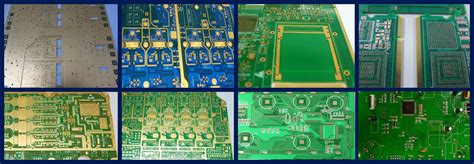
Printed Circuit Boards (PCBs) are essential components in modern electronics, forming the backbone of countless devices we use every day. PCB Manufacturers and fabricators, such as Neltec, play a crucial role in bringing these boards to life, ensuring they meet the highest quality standards and specifications. In this comprehensive article, we will explore the world of PCB manufacturing, focusing on Neltec’s expertise and the various aspects of the PCB fabrication process.
What are PCBs?
PCBs are thin boards made of insulating materials, such as fiberglass or composite epoxy, with conductive copper traces printed on them. These traces connect various electronic components, such as resistors, capacitors, and integrated circuits (ICs), to create a functional electronic circuit. PCBs come in different types, including:
- Single-sided PCBs
- Double-sided PCBs
- Multi-layer PCBs
- Flexible PCBs
- Rigid-flex PCBs
The Importance of PCB Manufacturers and Fabricators
PCB manufacturers and fabricators are responsible for transforming a PCB design into a physical board that can be used in electronic devices. They possess the expertise, equipment, and processes necessary to ensure that the final product meets the required specifications and performs as intended. Some of the key roles of PCB manufacturers and fabricators include:
- Advising on PCB design for manufacturability (DFM)
- Selecting appropriate materials based on the application
- Fabricating PCBs using state-of-the-art equipment and processes
- Conducting quality control and testing
- Providing support and guidance throughout the PCB development process
Neltec: A Leading PCB Manufacturer and Fabricator
Neltec is a renowned PCB manufacturer and fabricator, known for its commitment to quality, innovation, and customer satisfaction. With years of experience in the industry, Neltec has established itself as a trusted partner for businesses across various sectors, including telecommunications, automotive, medical, and aerospace.
Neltec’s Expertise and Capabilities
Neltec’s expertise in PCB manufacturing covers a wide range of technologies and applications. Some of their key capabilities include:
- High-density interconnect (HDI) PCBs
- Controlled impedance PCBs
- Thick Copper PCBs
- Microvia PCBs
- Blind and buried via PCBs
- Rigid-flex PCBs
- Metal-core PCBs
Neltec’s state-of-the-art facilities and equipment, combined with their skilled workforce, enable them to deliver high-quality PCBs consistently and efficiently.
Neltec’s Commitment to Quality and Customer Satisfaction
At Neltec, quality is not just a buzzword; it is a core value that permeates every aspect of their operations. The company adheres to strict quality control measures and industry standards, such as IPC and ISO, to ensure that every PCB they manufacture meets or exceeds customer expectations.
Neltec’s dedication to customer satisfaction is evident in their approach to communication, collaboration, and support. They work closely with their clients to understand their unique requirements and provide guidance throughout the PCB development process, from design to production and beyond.

The PCB Manufacturing Process
The PCB manufacturing process consists of several critical steps that transform a PCB design into a functional, physical board. Let’s take a closer look at each of these steps:
1. PCB Design and Preparation
The PCB manufacturing process begins with the PCB design. The design is created using specialized software, such as Altium Designer or KiCad, which allows engineers to lay out the circuit schematic and define the board’s physical dimensions, layer stackup, and component placement.
Once the design is complete, it is reviewed for manufacturability (DFM) to ensure that it can be efficiently and effectively produced. This review process helps identify and address any potential issues, such as insufficient clearances, improper routing, or incompatible materials.
2. Printing the Circuit Pattern
After the design is finalized and approved, the next step is to print the circuit pattern onto the PCB substrate. This process involves several sub-steps:
a. Copper Cladding
The PCB substrate, typically made of fiberglass or composite epoxy, is coated with a thin layer of copper on one or both sides, depending on the type of PCB being manufactured. This copper layer will form the basis for the circuit traces.
b. Applying the Photoresist
A photosensitive material called photoresist is applied to the copper-clad substrate. This material hardens when exposed to ultraviolet (UV) light, forming a protective layer over the copper.
c. Exposing the Photoresist
The PCB design is printed onto a transparent film, which is then placed on top of the photoresist-coated substrate. UV light is then applied, causing the photoresist to harden in the areas exposed through the transparent film.
d. Developing the Photoresist
The unexposed portions of the photoresist are removed using a chemical developer, leaving behind a precise pattern of hardened photoresist that corresponds to the PCB design.
3. Etching the Copper
With the photoresist pattern in place, the PCB is subjected to an etching process. An etchant, typically an acidic solution, is used to remove the exposed copper areas not protected by the hardened photoresist. This process leaves behind the copper traces that form the actual circuit pattern.
4. Removing the Photoresist
After etching, the hardened photoresist is no longer needed and is removed using a chemical stripper, revealing the copper traces beneath.
5. Drilling and Plating
Holes are drilled into the PCB to accommodate through-hole components and vias, which connect different layers of the board. These holes are then plated with copper to ensure electrical continuity.
6. Applying the Solder Mask
A solder mask, typically green in color, is applied to the PCB. This insulating layer helps protect the copper traces from oxidation and prevents solder bridges from forming during the soldering process. The solder mask also provides a clear indication of where components should be placed and soldered.
7. Silkscreening
The silkscreen layer is applied to the PCB, which includes text, logos, and other markings that aid in component placement and identification. This layer is typically white and is applied using a silkscreen printing process.
8. Surface Finish
A surface finish, such as HASL (Hot Air Solder Leveling), ENIG (Electroless Nickel Immersion Gold), or OSP (Organic Solderability Preservative), is applied to the exposed copper areas to protect them from oxidation and enhance solderability.
9. Electrical Testing
The manufactured PCBs undergo rigorous electrical testing to ensure that they function as intended and meet the specified requirements. This testing may include continuity tests, insulation resistance tests, and high-potential (hipot) tests.
10. Inspection and Quality Control
Throughout the manufacturing process, various inspections and quality control measures are implemented to identify and address any issues or defects. These may include visual inspections, automated optical inspection (AOI), and X-ray inspection for multi-layer boards.

Choosing the Right PCB Manufacturer and Fabricator
When selecting a PCB manufacturer and fabricator, it’s essential to consider several key factors to ensure that you receive high-quality PCBs that meet your specific requirements. Some of these factors include:
- Experience and expertise in your industry or application
- Quality control processes and certifications (e.g., ISO, IPC)
- Capability to handle your specific PCB requirements (e.g., HDI, controlled impedance)
- Turnaround time and delivery reliability
- Customer support and communication
- Pricing and value for money
Neltec excels in all these areas, making them a top choice for businesses seeking a reliable and experienced PCB manufacturer and fabricator.

The Future of PCB Manufacturing
As technology continues to advance, the demand for more complex, high-performance PCBs will only increase. PCB manufacturers and fabricators must stay at the forefront of these developments to remain competitive and meet the evolving needs of their customers.
Some of the emerging trends and technologies in PCB manufacturing include:
- Miniaturization and increased component density
- Adoption of advanced materials, such as ceramic and metal-core substrates
- Integration of embedded components and 3D printing techniques
- Increased use of automation and artificial intelligence (AI) in the manufacturing process
- Growing demand for eco-friendly and sustainable PCB solutions
Neltec is well-positioned to navigate these challenges and opportunities, thanks to their commitment to innovation, continuous improvement, and customer-centric approach.
Frequently Asked Questions (FAQ)
1. What is the typical turnaround time for PCB manufacturing?
The turnaround time for PCB manufacturing varies depending on the complexity of the design, the chosen manufacturer, and the specific requirements of the project. On average, standard PCBs can be manufactured within 5-10 business days, while more complex designs may take 2-3 weeks or longer.
2. What are the most common PCB surface finishes, and how do they differ?
The most common PCB surface finishes include HASL (Hot Air Solder Leveling), ENIG (Electroless Nickel Immersion Gold), and OSP (Organic Solderability Preservative). HASL is the most cost-effective option and provides good solderability, while ENIG offers excellent flatness and corrosion resistance. OSP is a more environmentally friendly option but has a shorter shelf life compared to HASL and ENIG.
3. What is the difference between a Prototype PCB and a production PCB?
Prototype PCBs are typically manufactured in small quantities (1-10 pieces) and are used for testing and validation purposes. They may not undergo the same level of quality control and inspection as production PCBs, which are manufactured in larger quantities and are intended for use in the final product.
4. How can I ensure that my PCB design is manufacturable?
To ensure that your PCB design is manufacturable, consider the following:
- Follow the manufacturer’s design guidelines and requirements
- Use standard component sizes and footprints
- Ensure adequate spacing between components and traces
- Avoid unnecessarily small features and hole sizes
- Conduct a design for manufacturability (DFM) review with your chosen manufacturer
5. What should I look for when selecting a PCB manufacturer and fabricator?
When selecting a PCB manufacturer and fabricator, consider their experience and expertise in your industry or application, quality control processes and certifications, capability to handle your specific PCB requirements, turnaround time and delivery reliability, customer support and communication, and pricing and value for money. Choosing a reputable manufacturer like Neltec can help ensure that you receive high-quality PCBs that meet your specific needs.
Conclusion
PCB manufacturing is a complex and critical process that requires expertise, precision, and attention to detail. PCB manufacturers and fabricators, such as Neltec, play a vital role in bringing electronic devices to life by transforming PCB designs into high-quality, functional boards.
By understanding the PCB manufacturing process, the importance of choosing the right manufacturer, and staying informed about emerging trends and technologies, businesses can make informed decisions and ensure the success of their electronic products.
Neltec’s commitment to quality, innovation, and customer satisfaction makes them a top choice for businesses seeking a reliable and experienced PCB manufacturer and fabricator. With their expertise and capabilities, Neltec is well-positioned to support the evolving needs of the electronics industry and contribute to the development of cutting-edge technologies.


Leave a Reply