What is the Definition of a PCB?
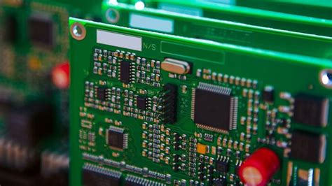
A PCB, or printed circuit board, is the foundation of nearly all modern electronic devices. PCBs are flat boards made of insulating materials with conductive copper traces, pads, and other features etched or printed on the surface. Components like integrated circuits, resistors, and capacitors are soldered onto the PCB to create a functional electronic circuit.
In simple terms, a PCB Definition is:
A thin board made of fiberglass or a similar insulating material with conductive pathways printed or etched on one or both sides. Electronic components are soldered to the PCB to create a working electronic product.
What is a PCB Used For?
PCBs are used in virtually all electronic devices today, providing both mechanical support and electrical interconnections for components. Some common applications of PCBs include:
- Computers and laptops
- Smartphones and tablets
- Televisions and displays
- Automotive electronics
- Medical devices
- Industrial control systems
- Aviation and aerospace electronics
- Consumer appliances
- IoT devices
PCBs enable the miniaturization and reliability of these electronic products by providing a compact, durable platform for circuits. They eliminate the need for bulky, unreliable point-to-point wiring.

What are the Different Types of PCBs?
There are several different types of PCBs, each with unique characteristics suited for different applications:
Single Layer PCBs
Single layer PCBs have conductive copper traces printed on one side of the insulating substrate. The components are soldered on the opposite side. Single layer PCBs are the simplest and most economical type, used for basic low-density circuits.
Double Layer PCBs
Double layer PCBs have conductive traces on both sides of the board. Through-hole vias are used to connect the circuits on the top and bottom layers. Double sided PCBs allow for higher component density and more complex circuits compared to single layer boards.
Multi-Layer PCBs
Multi-layer PCBs have three or more conductive copper layers laminated with insulating material in between. The inner layers allow circuits to cross over each other without intersecting. Multiple planes can be used for power and ground. High density interconnect (HDI) PCBs may have 8-12 layers or more. Multi-layer PCBs enable very high density, high speed circuits for advanced applications.
Rigid PCBs
Rigid PCBs use a solid, inflexible substrate material like fiberglass (FR4). This provides mechanical strength and stability. Rigid PCBs are the most common type used in electronic products.
Flexible PCBs
Flexible PCBs are made with flexible insulating plastic films like polyimide, with circuit traces printed on top. Flex PCBs can bend and flex to fit into tight spaces or movable parts. They are commonly used for connecting components in laptops, cameras, and medical devices.
Rigid-Flex PCBs
Rigid-flex PCBs combine flexible circuits and rigid circuits together in a single assembly. The rigid sections mount components while the flex sections act as interconnects between rigid boards. This enables high-density 3D configurations. Rigid-flex boards are used in aerospace, medical, and military applications.

What Materials are PCBs Made From?
PCBs are made from a combination of insulating substrate materials and conductive metal layers. The most common materials used in PCBs include:
PCB Substrate Materials
- FR4 fiberglass: glass-reinforced epoxy laminate, the most widely used
- Polyimide: high-temperature plastic film for flexible circuits
- Teflon: high-frequency, low-loss material for RF/microwave
- Ceramic: alumina or aluminum nitride for high-power circuits
- Metal core: aluminum or copper base for LED lighting PCBs
PCB Conductor Materials
- Copper foil: standard conductor material, may be plated with tin, nickel, gold
- Aluminum: low-cost for low-current applications
- Silver: for low-resistance circuits
- Carbon inks: for low-cost membrane switch and RFID antenna printing
The choice of PCB materials depends on the electrical, mechanical, and environmental requirements of the end application. Factors like operating temperature, dielectric constant, flexibility, and cost are considered.

How are PCBs Manufactured?
PCBs are manufactured through a multi-step process involving both additive and subtractive methods. The core steps in PCB fabrication are:
-
Design: The circuit schematic is captured and a PCB layout is created using EDA (electronic design automation) software.
-
Printing: The circuit pattern is printed onto the copper-clad laminate using photolithography. A photomask is used to transfer the circuit image to a light-sensitive resist coating on the copper.
-
Etching: The exposed copper not protected by the resist is chemically etched away, leaving only the desired circuit traces behind.
-
Drilling: Holes are drilled through the board to mount through-hole components or to create interconnecting vias between layers.
-
Plating: The holes are plated with copper to form conductive vias. Additional metal finishes like tin, nickel, or gold may be plated onto the copper traces.
-
Lamination: For multi-layer boards, additional insulating layers and copper foils are laminated together under high heat and pressure.
-
Solder Mask: A protective solder mask lacquer is applied over the outer copper layers, leaving only the component pads and testpoints exposed.
-
Silkscreen: A silkscreen legend is printed on the component side to label part numbers, testpoints, and other identifiers.
-
Surface Finish: The exposed pads are coated with a surface finish like HASL (hot air solder leveling), ENIG (electroless nickel immersion gold), or OSP (organic solderability preservative) to the pads to prevent oxidation and facilitate soldering.
-
Fabrication: The individual PCBs are routed out of the panel using a CNC milling machine or laser cutter.
-
Test: The finished PCBs are electrically tested using flying probe or Bed-of-Nails Testers to verify continuity and detect shorts or opens.
PCB Design Guidelines and Best Practices
Designing a PCB requires careful planning and adherence to best practices to ensure manufacturability, reliability, and functionality. Some key PCB design guidelines are:
Follow the Datasheet
Always refer to the component datasheets for recommended land patterns, pin assignments, and keepout areas. Use the suggested footprints unless there is a compelling reason to deviate.
Consider Manufacturability
Design your PCB with manufacturing in mind from the start. Follow the fabricator’s design rules for minimum trace/space width, hole size, and annular rings. Leave adequate space for assembly and test.
Use a Good Grid System
Establish a consistent grid system for component placement and routing. Common grid sizes are 25, 12.5, and 10 mils. A properly aligned grid will result in fewer off-grid errors and more efficient use of space.
Place Components Logically
Group components logically by function and place them to minimize connection lengths. Consider the flow of power and signals through the circuit. Place decoupling capacitors close to ICs.
Route Critical Traces First
Route the most critical and sensitive traces first, like clocks, high-speed signals, and analog paths. Give these traces priority for the optimal layer and path. Route high-current power traces wide and short.
Minimize Crosstalk
To minimize crosstalk between adjacent signals, route them on opposite sides of the board at 90 degree angles. Provide ground guards between sensitive traces. Avoid long parallel runs.
Optimize for EMC
To minimize EMI and improve signal integrity, use ground planes, bypass capacitors, and differential pair routing. Keep current loop areas small. Avoid slots or splits in ground/power planes.
Panelize for Assembly
If using automated assembly, panelize your PCBs to allow for efficient processing. Include fiducials, tooling holes, and breakaway tabs or mousebites in your panel design.
Check Your Design
Use your CAD tools’ DRC (Design Rule Check) and ERC (electrical rule check) to verify your design against manufacturing constraints and electrical rules. Perform a final design review before releasing to production.
Frequently Asked Questions about PCBs
What is the difference between a PCB and PCBA?
A PCB is the bare printed circuit board without components. A PCBA (printed circuit board assembly) is a PCB that has been populated with electronic components and soldered.
Are breadboards and PCBs the same?
No, breadboards and PCBs serve different purposes. A breadboard is a temporary prototyping tool for building and testing circuits. A PCB is a permanent, reliable platform for the final circuit.
Can a PCB be repaired?
Yes, PCBs can often be repaired by experienced technicians. Common PCB Repairs include resoldering broken joints, replacing damaged traces, and removing solder bridges. However, complex multi-layer boards may not be repairable.
How much do PCBs cost?
The cost of a PCB depends on the size, number of layers, materials, surface finish, and quantity. Simple 2-layer PCBs can cost under $1 each in volume. Large, complex boards with 8+ layers and special materials may cost $100 or more. Setup and tooling fees may also apply.
What is the typical turnaround time for PCB production?
Standard lead times for PCB fabrication are 1-2 weeks for prototypes and 3-4 weeks for production volumes. Expedited turns of 1-5 days are available from some suppliers at a higher cost. Lead times depend on the complexity, materials, and production queues.
Conclusion
In summary, a PCB is a fundamental building block of modern electronics that provides both structural support and electrical interconnectivity for components. Understanding what a PCB is, how they are made, and best design practices is essential for anyone involved in electronics design or manufacturing.
By following PCB design guidelines for manufacturability, signal integrity, and reliability, you can ensure your electronic products are functional, robust, and cost-effective. As PCB technology continues to evolve with new materials, processes, and design tools, the possibilities for innovative electronic products are endless.


Leave a Reply