Introduction to Circuit board design
Circuit board design is a critical aspect of electronic product development. A well-designed circuit board not only ensures the proper functioning of the device but also enhances its aesthetic appeal. In this comprehensive guide, we will explore the key elements of professional and beautiful circuit board design, providing you with the knowledge and tools to create stunning and functional circuit boards.
Understanding the Basics of Circuit Board Design
What is a Circuit Board?
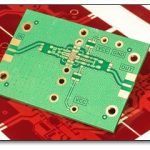
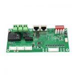
A circuit board, also known as a printed circuit board (PCB), is a flat board made of insulating material, such as fiberglass or plastic, with conductive tracks, pads, and other features etched onto its surface. It serves as the foundation for electronic components, providing electrical connections and mechanical support.
Types of Circuit Boards
There are several types of circuit boards, each with its own characteristics and applications:
| Type | Description | Application |
|---|---|---|
| Single-Sided PCB | Conductive tracks on one side only | Simple, low-cost devices |
| Double-sided PCB | Conductive tracks on both sides | More complex devices |
| Multi-layer PCB | Multiple layers of conductive tracks | High-density, complex devices |
| Flexible PCB | Flexible substrate material | Wearable electronics, tight spaces |
| Rigid-Flex PCB | Combination of rigid and flexible sections | Devices requiring both stability and flexibility |
Circuit Board Materials
The choice of material for your circuit board depends on various factors, such as the intended application, environmental conditions, and budget. Common materials include:
- FR-4: A flame-retardant fiberglass-reinforced epoxy laminate, widely used for its durability and low cost.
- Polyimide: A flexible, heat-resistant material suitable for high-temperature applications and Flexible PCBs.
- Aluminum: Used as a substrate for high-power applications, offering excellent thermal dissipation properties.
Designing Your Circuit Board Layout
Schematic Design
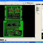
Before starting the physical layout of your circuit board, create a schematic diagram that represents the electrical connections between components. Use a schematic capture tool to create a clear and organized diagram, following best practices for symbol placement, labeling, and net naming.
Component Placement
Once you have a schematic, begin placing components on the virtual circuit board. Consider the following factors:
- Functional grouping: Place related components close together to minimize signal path lengths and improve performance.
- Thermal management: Position heat-generating components away from sensitive devices and provide adequate cooling.
- Mechanical constraints: Consider the physical dimensions of components and ensure proper clearance for assembly and enclosure fit.
Routing and Trace Width
When routing the connections between components, follow these guidelines:
- Use appropriate trace widths based on the expected current flow and manufacturing capabilities.
- Minimize trace lengths to reduce signal delay and noise.
- Avoid sharp angles and provide smooth transitions for traces.
- Maintain proper spacing between traces to prevent signal interference and manufacturability issues.
Ground and Power Planes
Incorporate ground and power planes in your circuit board design to provide low-impedance paths for current flow and reduce noise. Use solid copper fills for these planes, and consider split planes for separate analog and digital sections if necessary.
Electromagnetic Compatibility (EMC)
To minimize electromagnetic interference (EMI) and ensure compliance with EMC regulations, follow these practices:
- Use proper grounding techniques, such as a single-point ground or star grounding.
- Implement shielding for sensitive components or high-frequency signals.
- Apply filtering techniques, such as decoupling capacitors and ferrite beads, to suppress noise.

Aesthetics and Visual Appeal
Color and Finish
Choose an appropriate color and finish for your circuit board to enhance its visual appeal. Common options include:
- Green: The traditional color for PCBs, providing good contrast for component markings.
- Black: A sleek and modern choice, often used for high-end devices.
- White: Offers a clean and minimalist look, suitable for LED lighting applications.
- Matte or glossy finish: Matte finish reduces glare, while glossy finish provides a polished appearance.
Silkscreen and Labeling
Use silkscreen printing to add labels, logos, and other information to your circuit board. Consider the following tips:
- Use clear and legible fonts for component labels and values.
- Include polarity markers and pin numbers for easy assembly and troubleshooting.
- Add your company logo or product branding for a professional touch.
Copper Pours and Artistic Patterns
Incorporate copper pours and artistic patterns into your circuit board design to create a unique and visually striking appearance. Use solid copper fills for unused areas, and experiment with creative shapes and designs that complement your product’s aesthetics.
Manufacturing Considerations
Design for Manufacturing (DFM)
To ensure the manufacturability of your circuit board, adhere to the following DFM guidelines:
- Follow the minimum trace width and spacing requirements specified by your manufacturer.
- Use standard component sizes and footprints to avoid custom tooling costs.
- Provide adequate clearance around components for automated assembly processes.
Panelization and Breakaway Tabs
If producing multiple circuit boards in a single manufacturing run, use panelization to arrange them in a larger panel. Include breakaway tabs or mouse bites to facilitate easy separation of individual boards after fabrication.
Documentation and Files
Prepare a comprehensive set of documentation and files for your manufacturer, including:
- Gerber files: Industry-standard format for conveying PCB design information.
- Drill files: Specifies the location and size of holes on the circuit board.
- Bill of Materials (BOM): A list of all components used in the design, including quantities and part numbers.
- Assembly drawings: Provides visual guidance for component placement and orientation.
Frequently Asked Questions (FAQ)
-
What software tools are commonly used for circuit board design?
Popular software tools for circuit board design include Altium Designer, KiCad, Eagle, and OrCAD. These tools offer schematic capture, PCB layout, and 3D visualization capabilities. -
How do I choose the right layer count for my circuit board?
The layer count depends on the complexity of your design and the required functionality. Simple designs can use single or double-sided boards, while complex designs with high component density may require multi-layer boards. Consider factors such as signal integrity, power distribution, and manufacturing costs when deciding on the layer count. -
What are the benefits of using a four-layer circuit board?
Four-layer circuit boards offer several benefits over two-layer boards: - Improved signal integrity and reduced noise due to dedicated ground and power planes.
- Better EMI performance by providing shielding between layers.
- Increased routing flexibility and component density.
-
Enhanced mechanical stability and durability.
-
How can I ensure the reliability of my circuit board design?
To ensure the reliability of your circuit board design: - Follow best practices for component placement, routing, and grounding.
- Use appropriate trace widths and spacing based on current requirements and manufacturing capabilities.
- Implement proper thermal management techniques to prevent overheating.
-
Conduct thorough testing and validation, including environmental stress tests and accelerated life tests.
-
What are the common pitfalls to avoid in circuit board design?
Common pitfalls to avoid in circuit board design include: - Neglecting to consider manufacturing constraints and DFM guidelines.
- Inadequate power distribution and grounding, leading to noise and signal integrity issues.
- Poor component placement and routing, resulting in signal crosstalk and EMI problems.
- Overlooking thermal management and failing to provide proper cooling for heat-generating components.
- Insufficient documentation and communication with the manufacturing team.
Conclusion
Designing a professional and beautiful circuit board requires a combination of technical expertise, attention to detail, and aesthetic sensibility. By understanding the basics of circuit board design, following best practices for layout and routing, and incorporating visual appeal through color, silkscreen, and artistic patterns, you can create circuit boards that are both functional and visually stunning.
Remember to consider manufacturing constraints, conduct thorough testing and validation, and provide comprehensive documentation to ensure a smooth and successful production process. With practice and experience, you can master the art of circuit board design and bring your electronic products to life with style and sophistication.


Leave a Reply