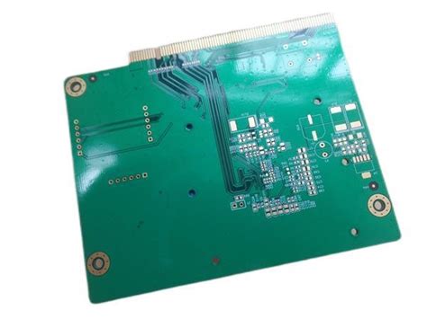
What are PCB Gold Fingers?
PCB Gold Fingers, also known as edge connectors or contact fingers, are the gold-plated pads or traces located on the edge of a printed circuit board (PCB). These conductive surfaces are designed to connect the PCB to other devices or systems, such as connectors, sockets, or slots. Gold fingers are commonly found on various types of PCBs, including computer peripherals, expansion cards, and memory modules.
Key Characteristics of PCB Gold Fingers
-
Material: Gold fingers are typically made of copper with a layer of nickel plating, followed by a thin layer of gold plating. The gold plating provides excellent conductivity, corrosion resistance, and durability.
-
Thickness: The thickness of the gold plating on PCB fingers can vary depending on the application and requirements. Common thicknesses range from 0.05 microns to 2.54 microns (1-100 microinches).
-
Pitch: The pitch, or the distance between the center of one gold finger to the center of the adjacent finger, is an essential factor in designing PCB gold fingers. Common pitches include 1.27 mm, 2.54 mm, and 3.96 mm.
-
Dimensions: The length and width of gold fingers depend on the specific application and the size of the PCB. Typical lengths range from 10 mm to 80 mm, while widths can vary from 1 mm to 3 mm.
Advantages of Using PCB Gold Fingers
1. Excellent Conductivity
Gold is an excellent conductor of electricity, making it an ideal material for creating reliable connections between PCBs and other components. The high conductivity of gold ensures minimal signal loss and optimal performance in electronic devices.
2. Corrosion Resistance
Gold is highly resistant to corrosion and oxidation, which helps maintain the integrity of the electrical connections over time. This is particularly important in harsh environments or applications where the PCB may be exposed to moisture, humidity, or other corrosive elements.
3. Durability and Longevity
PCB gold fingers are designed to withstand numerous insertion and removal cycles without significant wear or damage. The hardness and abrasion resistance of the gold plating contribute to the longevity of the connectors, ensuring reliable connections even after repeated use.
4. Compatibility with Various Connectors
Gold fingers are compatible with a wide range of connectors, sockets, and slots used in electronic devices. This compatibility allows for seamless integration of PCBs into different systems and enables easy upgrades or replacements when necessary.

Applications of PCB Gold Fingers
PCB gold fingers find applications in various industries and products, including:
-
Computer Hardware: Expansion cards, graphics cards, and memory modules (e.g., RAM, SSD) use gold fingers to connect to the motherboard.
-
Consumer Electronics: Many electronic devices, such as smartphones, tablets, and digital cameras, use PCBs with gold fingers for connecting components like displays, batteries, or storage.
-
Industrial Equipment: PCBs with gold fingers are used in industrial control systems, automation devices, and test and measurement equipment.
-
Medical Devices: Medical equipment, such as patient monitors, diagnostic tools, and imaging systems, often incorporate PCBs with gold fingers for reliable connections.
-
Automotive Electronics: PCBs with gold fingers are used in various automotive applications, including infotainment systems, sensors, and control units.

Designing PCB Gold Fingers
When designing PCB gold fingers, several factors need to be considered to ensure optimal performance and reliability:
1. Finger Dimensions
The length, width, and pitch of the gold fingers should be determined based on the specific application and the mating connector requirements. Proper dimensioning ensures a secure and reliable connection between the PCB and the connector.
2. Plating Thickness
The thickness of the gold plating on the fingers should be specified based on the expected number of mating cycles and the environment in which the PCB will be used. Thicker plating provides better wear resistance and longevity but may increase costs.
3. Solder Mask Design
A solder mask is often applied to the PCB to protect the circuitry and prevent short circuits. When designing gold fingers, it is crucial to ensure that the solder mask is properly aligned and does not overlap with the fingers, as this can interfere with the connection.
4. Impedance Control
For high-speed or high-frequency applications, it is essential to consider the impedance of the gold fingers and ensure that it matches the impedance of the mating connector and the PCB traces. Proper impedance matching minimizes signal reflections and ensures optimal signal integrity.

Manufacturing PCB Gold Fingers
The manufacturing process for PCB gold fingers involves several steps:
-
PCB Fabrication: The PCB is fabricated using standard PCB manufacturing techniques, such as etching, drilling, and lamination.
-
Nickel Plating: A layer of nickel is plated onto the copper fingers to provide a barrier between the copper and the gold plating. Nickel also enhances the adhesion of the gold layer and improves wear resistance.
-
Gold Plating: The nickel-plated fingers are then plated with a thin layer of gold using electroplating or immersion plating techniques. The thickness of the gold plating is controlled to meet the specified requirements.
-
Solder Mask Application: A solder mask is applied to the PCB, covering the areas around the gold fingers while leaving the fingers exposed for connection.
-
Surface Finish: The exposed gold fingers may undergo additional surface finishing processes, such as chemical or mechanical cleaning, to remove any contaminants and ensure optimal contact performance.
Testing and Quality Control
To ensure the reliability and performance of PCB gold fingers, various tests and quality control measures are employed during the manufacturing process:
-
Visual Inspection: The gold fingers are visually inspected for any defects, such as scratches, pits, or contamination.
-
Thickness Measurement: The thickness of the gold plating is measured using X-ray fluorescence (XRF) or other non-destructive techniques to ensure compliance with the specified requirements.
-
Adhesion Test: The adhesion of the gold plating to the underlying nickel and copper layers is tested using tape tests or peel tests to ensure adequate bonding strength.
-
Continuity and Resistance Test: Electrical continuity and resistance tests are performed to verify that the gold fingers provide reliable electrical connections with low resistance.
-
Environmental Testing: PCBs with gold fingers may be subjected to environmental tests, such as temperature cycling, humidity exposure, or salt spray tests, to evaluate their performance and durability under different conditions.
Frequently Asked Questions (FAQ)
1. What is the purpose of nickel plating under the gold plating on PCB fingers?
Nickel plating serves two main purposes: it provides a barrier layer between the copper and the gold to prevent the formation of intermetallic compounds, and it enhances the adhesion of the gold layer to the copper substrate. Additionally, nickel plating improves the wear resistance of the gold fingers.
2. Can PCB gold fingers be repaired if damaged?
In most cases, damaged PCB gold fingers cannot be easily repaired. Attempts to repair gold fingers may result in further damage to the PCB or compromised connection reliability. If the gold fingers are severely damaged, the best course of action is to replace the entire PCB.
3. How does the thickness of the gold plating affect the performance of PCB fingers?
Thicker gold plating provides better wear resistance and longevity, especially in applications with frequent mating cycles. However, thicker plating also increases the cost of the PCB. The choice of plating thickness should be based on the specific requirements of the application, considering factors such as the expected number of mating cycles and the operating environment.
4. Are there alternatives to gold plating for PCB fingers?
While gold plating is the most common choice for PCB fingers due to its excellent conductivity and corrosion resistance, there are some alternatives. These include silver plating, palladium plating, and gold-flash over nickel plating. However, these alternatives may not provide the same level of performance and reliability as gold plating, especially in demanding applications.
5. How can I ensure the compatibility of PCB gold fingers with mating connectors?
To ensure compatibility between PCB gold fingers and mating connectors, it is essential to adhere to industry standards and specifications for connector design, such as those provided by organizations like IPC (Association Connecting Electronics Industries) or JEDEC (Joint Electron Device Engineering Council). Following these standards helps ensure interoperability and reliability in the final application.
| Plating Thickness | Common Applications |
|---|---|
| 0.05 – 0.25 microns | Low-cost consumer electronics, short mating cycles |
| 0.25 – 1.27 microns | Moderate mating cycles, general-purpose applications |
| 1.27 – 2.54 microns | High mating cycles, industrial and automotive applications |
| Pitch (mm) | Common Applications |
|---|---|
| 1.27 | Compact PCBs, high-density connectors |
| 2.54 | General-purpose PCBs, standard connectors |
| 3.96 | High-power applications, larger connectors |
In conclusion, PCB gold fingers play a crucial role in ensuring reliable and durable connections between PCBs and other components in various electronic devices. By understanding the key characteristics, advantages, and design considerations of gold fingers, engineers and manufacturers can create PCBs that meet the specific requirements of their applications while ensuring optimal performance and longevity.


Leave a Reply