Introduction
Designing and laying out a printed circuit board (PCB) for an audio amplifier requires careful consideration of many factors to achieve optimal performance, reliability, and immunity to radio frequency (RF) interference. RF noise can couple into sensitive audio circuitry and cause distortion, hum, and other unwanted artifacts that degrade sound quality. By following best practices for component placement, routing, grounding, and shielding, you can create an RF-Immune PCB that delivers clean, noise-free amplification.
In this article, we will dive deep into the techniques and strategies for designing an audio amplifier PCB with high RF immunity. We’ll cover:
- Understanding sources of RF noise and coupling mechanisms
- Component selection and placement
- Power supply routing and decoupling
- Signal routing and layer stackup
- Ground planes and grounding strategies
- Shielding and filtering techniques
- PCB materials and manufacturing considerations
By the end, you’ll have a solid foundation for tackling your next RF-immune audio amplifier PCB design. Let’s get started!
Understanding RF Noise and Coupling
Before we get into PCB layout techniques, it’s important to understand the nature of RF noise and how it can make its way into an audio circuit. RF interference can be radiated from external sources like cell phones, Wi-Fi routers, and radio transmitters, or it can be generated internally by high-speed digital circuitry, switch-mode power supplies, and other noisy components.
There are three main coupling mechanisms that allow RF energy to enter a circuit:
- Conducted coupling – RF noise travels along power supply rails, ground paths, and signal traces.
- Radiated coupling – RF fields induce currents in PCB traces, component leads, and cables.
- Capacitive/inductive coupling – Stray Capacitance and mutual inductance provide paths for RF noise to jump between circuit nodes.
To achieve RF immunity, the PCB layout must be designed to minimize the effects of all three coupling mechanisms. This requires careful component placement, routing, grounding, and shielding, as we’ll see in the following sections.
Component Selection and Placement
The first step in creating an RF-immune PCB is selecting components that are inherently resistant to RF interference. This includes:
- Using metal film resistors instead of carbon composition types
- Using RF-suppressive ferrite beads for power supply filtering
- Choosing capacitors with low equivalent series resistance (ESR) and self-resonant frequencies (SRF) above the frequencies of concern
- Using shielded inductors or toroids for power supply filtering
- Selecting op-amps and other ICs with good power supply rejection ratio (PSRR) and common-mode rejection ratio (CMRR)
Once the components are selected, they must be placed on the PCB in a way that minimizes coupling and interaction. Here are some guidelines to follow:
- Physically separate sensitive analog circuitry from noisy digital sections. Use separate ground planes if possible.
- Keep high-impedance nodes (op-amp inputs) away from strong RF fields. Consider shielding if necessary.
- Locate decoupling capacitors as close as possible to IC power pins.
- Avoid placing inductors and transformers near each other to minimize mutual coupling.
- Orient components to minimize coupling between adjacent pins and traces.
- Minimize trace lengths, especially for high-impedance and RF-sensitive signals.
By carefully selecting and placing components, you can create a solid foundation for an RF-resistant PCB layout.

Power Supply Routing and Decoupling
The power supply is a common entry point for RF noise, so it’s critical to design a robust power delivery network (PDN) that minimizes conducted and radiated interference. Here are some key techniques:
- Use separate analog and digital power supplies if possible, with their own decoupling networks.
- Route power traces on inner layers, sandwiched between ground planes for shielding.
- Use wide, low-impedance traces for power distribution to minimize IR drops and voltage gradients that can couple noise.
- Decouple ICs with ceramics caps (0.1uF – 0.01uF) placed close to power pins to shunt high frequency noise.
- Use bulk decoupling with electrolytic caps (1uF – 100uF) near Voltage Regulators to stabilize DC supply.
- Consider LC or RC power supply filtering for sensitive analog circuits.
- Use a star grounding topology originating from a single point near the power input.
Here’s an example of a good decoupling scheme for an op-amp:
The 0.1uF and 10uF caps shunt RF noise to ground at the power pins, while the ferrite bead isolates the op-amp supply from the rest of the circuit. The 10uF cap stabilizes the local supply voltage.
Signal Routing and Layer Stackup
Proper signal routing is key to minimizing radiated and capacitively-coupled RF interference. Here are some guidelines to follow:
- Route sensitive analog signals on inner layers, sandwiched between ground planes for shielding.
- Avoid routing signals parallel to each other for long distances to minimize crosstalk.
- Keep digital and analog signals separated as much as possible.
- Minimize trace lengths and use direct routing paths.
- Avoid routing traces under noisy components like power supplies.
- Use ground guard traces to isolate sensitive signals.
- Terminate unused IC pins and connectors to ground.
The layer stackup should be designed to provide a low-impedance return path for high-frequency currents and to minimize radiated emissions. A typical 4-layer stackup for an RF-immune audio PCB might look like this:
| Layer | Content |
|---|---|
| Top | Components, power, high-speed digital |
| GND | Solid ground plane |
| PWR | Power planes and low-speed signals |
| Bottom | Components, sensitive analog, RF |
The internal ground layer provides shielding between the power/digital and analog/RF layers. Additional layers can be added as needed to accommodate more complex routing.
Grounding Strategies
A properly designed grounding scheme is perhaps the most important aspect of RF immunity. The goal is to provide a low-impedance return path for RF currents while minimizing ground loops and voltage gradients that can couple noise. Here are some key grounding techniques:
- Use a solid ground plane on one or more layers, with no splits or cuts.
- Connect all ground pins directly to the ground plane with short, wide traces or vias.
- Use a star grounding topology for analog circuits, with a single point ground near the power input.
- Separate analog and digital grounds, joining them at a single point near the power input.
- Avoid daisy-chaining ground connections, which can create ground loops.
- Use multiple vias to stitch ground planes together at frequent intervals.
- Avoid slots or gaps in ground planes, which can act as antennas.
Here’s an example of a good grounding scheme for an audio amplifier:
The analog and digital grounds are separated, with a single point connection near the power input. All ground pins are connected directly to their respective ground planes. Multiple vias stitch the top and bottom ground planes together.
Shielding and Filtering
In some cases, proper layout techniques alone may not be enough to achieve adequate RF immunity. Additional shielding and filtering may be necessary to further reduce interference. Here are some options to consider:
- Use shielded cables for inputs and outputs, with the shield grounded at one end.
- Add metal shields over sensitive analog components or entire circuit sections. Connect shields to ground with multiple vias.
- Use feed-through or multilayer ceramic capacitors for filtered connectors.
- Add RC or LC filters to sensitive analog inputs.
- Use common-mode chokes on differential signal pairs.
- Consider adding a shielding layer (e.g. copper foil) to the PCB Stackup.
Here’s an example of an LC filter for an analog input:
The series inductor and shunt capacitor form a low-pass filter that attenuates RF noise while allowing the desired audio signal to pass through. The ferrite bead provides additional high-frequency filtering.
PCB Materials and Manufacturing
The choice of PCB materials and manufacturing processes can also impact RF immunity. Here are some factors to consider:
- Use high-quality, low-loss PCB Substrates like FR-4 or Rogers materials.
- Specify tighter tolerances for trace width, spacing, and via size to ensure consistent impedance and minimize RF leakage.
- Consider using thicker copper layers (2oz or more) for power and ground planes to lower impedance.
- Use immersion silver or gold plating instead of HASL for better high-frequency performance.
- Specify a smooth, uniform soldermask to minimize capacitive coupling between traces.
- Consider using a Conformal Coating to protect against moisture and contaminants that can degrade RF performance over time.
By carefully selecting materials and specifying manufacturing requirements, you can ensure that your PCB will perform well in an RF environment.
Frequently Asked Questions
Q: How important is the PCB layer stackup for RF immunity?
A: The layer stackup is critical for RF immunity, as it determines the effectiveness of shielding, grounding, and signal routing. A good stackup should have one or more solid ground planes, with sensitive signals routed on inner layers away from sources of interference. The stackup should also provide a low-impedance return path for high-frequency currents.
Q: Can I use a two-layer PCB for an RF-immune audio amplifier?
A: While it’s possible to design an RF-resistant audio amplifier on a two-layer PCB, it’s much more challenging than using a four-layer or higher stackup. With only two layers, it’s difficult to provide effective shielding and grounding, and signal routing options are limited. For best results, it’s recommended to use at least a four-layer PCB with dedicated ground and power planes.
Q: How do I choose the right decoupling capacitors for my audio amplifier?
A: Decoupling capacitors should be chosen based on their frequency response and impedance characteristics. For high-frequency decoupling, use ceramic capacitors with low ESR and SRF above the frequency range of concern. For bulk decoupling, use larger electrolytic or tantalum capacitors with good low-frequency performance. It’s also important to choose capacitors with voltage ratings above the expected supply voltage, and to use multiple capacitors in parallel to reduce the overall impedance.
Q: What are some common mistakes to avoid when routing signals on an RF-immune PCB?
A: Some common routing mistakes include:
- Running sensitive signals too close to noisy digital or power traces
- Routing signals parallel to each other for long distances, which can cause crosstalk
- Using long, meandering traces instead of direct paths
- Failing to provide an adequate ground return path for high-frequency signals
- Routing traces under noisy components like power supplies or high-speed digital ICs
- Not using ground guard traces or shielding for sensitive signals
By avoiding these mistakes and following best practices for signal routing, you can minimize the risk of RF interference and ensure good performance.
Q: How can I test the RF immunity of my audio amplifier PCB?
A: There are several ways to test the RF immunity of an audio amplifier PCB:
- Use an RF signal generator and injection probe to introduce RF noise into various points on the PCB, and monitor the output for any degradation in performance.
- Place the PCB in an anechoic chamber or shielded enclosure and measure its radiated emissions with an RF spectrum analyzer.
- Use an RF near-field probe to scan the PCB for areas of high RF leakage or coupling.
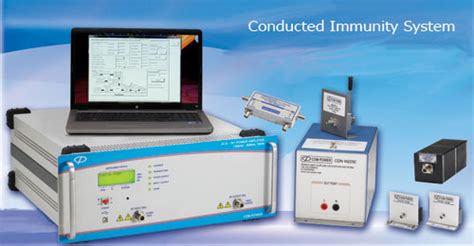
- Conduct immunity testing per industry standards like IEC 61000-4-3 (radiated immunity) or IEC 61000-4-6 (conducted immunity).
By performing these tests and analyzing the results, you can identify any weaknesses in your PCB design and take steps to improve its RF immunity.
Conclusion
Designing an RF-immune PCB for an audio amplifier requires careful attention to every aspect of the layout, from component selection and placement to routing, grounding, and shielding. By following the techniques and best practices outlined in this article, you can create a PCB that delivers clean, noise-free audio performance even in the presence of RF interference.
Remember to:
- Select components that are inherently resistant to RF noise
- Place components carefully to minimize coupling and interaction
- Use separate analog and digital power supplies with proper decoupling
- Route sensitive signals on inner layers with solid ground planes for shielding
- Use a star grounding topology with separate analog and digital grounds
- Add shielding and filtering as needed to further reduce interference
- Choose high-quality PCB materials and specify tight manufacturing tolerances
With these guidelines in mind, you’ll be well on your way to designing an RF-immune audio amplifier PCB that sounds great and stands up to the toughest RF environments.
Leave a Reply