What are PCB Drilled Holes?
PCB drilled holes are openings created in a printed circuit board using a drilling process. These holes are typically made using specialized drilling machines that can create precise and consistent openings in the PCB material. The holes can vary in size, shape, and location depending on the specific requirements of the PCB design.
Types of PCB Drilled Holes
There are several types of PCB drilled holes, each serving a specific purpose in the overall design and functionality of the circuit board. The main types of PCB drilled holes include:
- Through Holes
- Blind Vias
- Buried Vias
- Micro Vias
- Countersunk Holes
- Tooling Holes
1. Through Holes
Through holes are the most common type of PCB drilled holes. As the name suggests, these holes go completely through the PCB, from one side to the other. Through holes are used for several purposes, including:
- Mounting through-hole components
- Creating electrical connections between layers
- Providing mechanical support and stability
Through holes are typically plated with a conductive material, such as copper, to ensure reliable electrical connections between the layers of the PCB.
| Characteristic | Description |
|---|---|
| Hole Diameter | Typically 0.5 mm to 1.0 mm |
| Plating | Copper |
| Purpose | Component mounting, inter-layer connections, mechanical support |
2. Blind Vias
Blind vias are holes that start from one side of the PCB and terminate at a specific inner layer, without reaching the opposite side of the board. These holes are used to create electrical connections between the surface layer and one or more inner layers of the PCB. Blind vias are commonly used in high-density PCB designs where space is limited.
| Characteristic | Description |
|---|---|
| Hole Depth | Starts from one side and ends at a specific inner layer |
| Plating | Copper |
| Purpose | Electrical connections between surface and inner layers |
3. Buried Vias
Buried vias are holes that are located entirely within the inner layers of the PCB, without extending to either surface of the board. These holes are used to create electrical connections between the inner layers of the PCB. Buried vias are typically used in complex, multi-layer PCB designs to optimize space and improve signal integrity.
| Characteristic | Description |
|---|---|
| Hole Location | Entirely within inner layers |
| Plating | Copper |
| Purpose | Electrical connections between inner layers |
4. Micro Vias
Micro vias are small, high-precision drilled holes used in high-density PCB designs. These holes typically have a diameter of 0.15 mm or less and are used to create electrical connections between adjacent layers in the PCB. Micro vias are essential for advanced packaging technologies, such as chip-scale packaging (CSP) and ball grid arrays (BGA).
| Characteristic | Description |
|---|---|
| Hole Diameter | 0.15 mm or less |
| Plating | Copper |
| Purpose | Electrical connections between adjacent layers in high-density designs |
5. Countersunk Holes
Countersunk holes are drilled holes with a specially shaped opening that allows the head of a screw or bolt to sit flush with the surface of the PCB. These holes are used for mounting purposes, particularly when a low-profile or flush surface is required. Countersunk holes are commonly used for mounting PCBs to enclosures or other mechanical components.
| Characteristic | Description |
|---|---|
| Hole Shape | Tapered opening to accommodate screw or bolt head |
| Plating | Optional, depending on application |
| Purpose | Mounting PCBs with a flush surface |
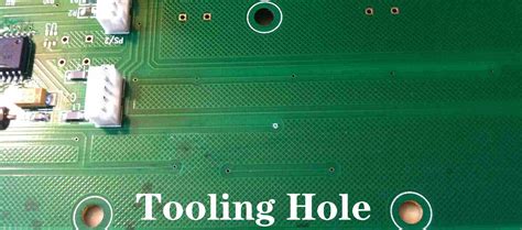
6. Tooling Holes
Tooling holes are non-functional holes drilled in a PCB for manufacturing and assembly purposes. These holes are used for aligning and securing the PCB during the fabrication process, as well as for mounting the board during the assembly of the final product. Tooling holes are typically located in the corners or edges of the PCB and do not have any electrical functionality.
| Characteristic | Description |
|---|---|
| Hole Location | Corners or edges of the PCB |
| Plating | Not required |
| Purpose | Alignment and securing during manufacturing and assembly |
PCB Drilled Hole Design Considerations
When designing PCBs with drilled holes, several factors must be considered to ensure optimal performance and manufacturability. Some of the key design considerations include:
1. Hole Size and Tolerance
The size of the drilled holes should be carefully chosen based on the components being used and the manufacturing capabilities of the PCB fabricator. It is essential to specify the appropriate hole size and tolerance to ensure proper fit and function of the components.
2. Annular Ring
The annular ring is the copper pad surrounding a drilled hole on a PCB. The annular ring provides a reliable electrical connection between the hole and the surrounding copper traces. It is crucial to maintain a sufficient annular ring width to ensure the structural integrity of the hole and to prevent any breakage during the manufacturing process.
3. Hole-to-Hole Spacing
The spacing between drilled holes should be carefully considered to avoid any potential manufacturing issues or signal integrity problems. Adequate hole-to-hole spacing helps prevent drilling errors and ensures that the PCB can be manufactured reliably.
4. Layer Stack-Up
The arrangement of the layers in a multi-layer PCB, known as the layer stack-up, plays a significant role in the design of drilled holes. The stack-up determines the location and type of drilled holes that can be used, as well as their impact on signal integrity and power distribution.
5. High-Speed Design Considerations
In high-speed PCB designs, the placement and type of drilled holes can have a significant impact on signal integrity. Factors such as hole size, location, and plating should be carefully considered to minimize signal reflections, crosstalk, and other signal integrity issues.

FAQ
1. What is the difference between a through hole and a via?
A through hole is a drilled hole that goes completely through the PCB, while a via is a drilled hole that is used to create an electrical connection between layers. Vias can be blind (starting from one side and terminating at an inner layer), buried (located entirely within inner layers), or through (extending from one side to the other).
2. Can drilled holes be used for component mounting?
Yes, through holes are commonly used for mounting through-hole components on a PCB. The holes are typically plated with a conductive material to ensure a reliable electrical connection between the component leads and the PCB Traces.
3. What is the purpose of tooling holes in a PCB?
Tooling holes are non-functional holes drilled in a PCB for manufacturing and assembly purposes. They are used for aligning and securing the PCB during the fabrication process and for mounting the board during the assembly of the final product.
4. How small can micro vias be?
Micro vias typically have a diameter of 0.15 mm or less. These small, high-precision drilled holes are used in high-density PCB designs to create electrical connections between adjacent layers.
5. Why are countersunk holes used in PCBs?
Countersunk holes are used for mounting purposes, particularly when a low-profile or flush surface is required. These holes have a specially shaped opening that allows the head of a screw or bolt to sit flush with the surface of the PCB, making them ideal for mounting PCBs to enclosures or other mechanical components.

Conclusion
PCB drilled holes are an essential aspect of printed Circuit Board Design and manufacturing. The various types of drilled holes, including through holes, blind vias, buried vias, micro vias, countersunk holes, and tooling holes, serve specific purposes in the overall functionality and performance of the PCB.
When designing PCBs with drilled holes, it is crucial to consider factors such as hole size and tolerance, annular ring width, hole-to-hole spacing, layer stack-up, and high-speed design considerations. By carefully addressing these design aspects, engineers can ensure that their PCBs are manufacturable, reliable, and meet the required performance specifications.
As PCB technology continues to advance, the importance of drilled holes in enabling high-density designs and advanced packaging technologies will only continue to grow. Understanding the types and applications of PCB drilled holes is essential for anyone involved in the design, manufacture, or assembly of electronic devices.


Leave a Reply