Introduction to PCB Drilled Holes
Printed Circuit Boards (PCBs) are essential components in modern electronics. They provide a platform for mounting and connecting electronic components, allowing for the creation of complex circuits. One crucial aspect of PCB design and manufacturing is the incorporation of drilled holes. These holes serve various purposes, such as allowing for the insertion of through-hole components, providing electrical connections between layers, and enabling the attachment of the PCB to other parts of the device.
In this comprehensive article, we will delve into the world of PCB drilled holes, covering everything you need to know to avoid surprises during the design and manufacturing process. We will discuss the different types of drilled holes, their functions, design considerations, manufacturing processes, and common issues that may arise.
Types of PCB Drilled Holes
There are several types of drilled holes used in PCBs, each serving a specific purpose. Let’s take a closer look at the most common types:
Through Holes
Through holes are the most basic type of drilled holes in PCBs. They extend completely through the board, from one side to the other. These holes are typically used for mounting through-hole components, such as resistors, capacitors, and connectors. They also allow for electrical connections between layers of the PCB.
Blind Vias
Blind vias are drilled holes that start from one side of the PCB and terminate at a specific inner layer, without extending to the opposite side of the board. They are used to create connections between the outer layer and one or more inner layers of the PCB. Blind vias are particularly useful in high-density designs where space is limited.
Buried Vias
Buried vias are drilled holes that connect two or more inner layers of the PCB without extending to either of the outer layers. They are used to create connections between inner layers, allowing for more complex routing and increased circuit density. Buried vias are typically used in multi-layer PCBs with four or more layers.
Micro Vias
Micro vias are small-diameter drilled holes, typically less than 0.15mm (6 mils) in diameter. They are used for high-density interconnects, especially in HDI (High-Density Interconnect) PCBs. Micro vias can be created using laser drilling or controlled depth drilling techniques, allowing for precise and reliable connections between layers.

Functions of PCB Drilled Holes
PCB drilled holes serve several critical functions in the design and operation of electronic devices. Let’s explore the main functions of these holes:
Component Mounting
One of the primary functions of drilled holes in PCBs is to allow for the mounting of through-hole components. These components have leads that are inserted into the holes and soldered in place, creating a strong mechanical and electrical connection. Through-hole mounting provides a robust and reliable method for attaching components to the PCB.
Electrical Connections
Drilled holes also play a vital role in establishing electrical connections between layers of the PCB. By using vias (through holes, blind vias, or buried vias), designers can route signals and power between different layers of the board, creating a three-dimensional circuit. This allows for more efficient use of space and enables the creation of complex, high-density designs.
Mechanical Support
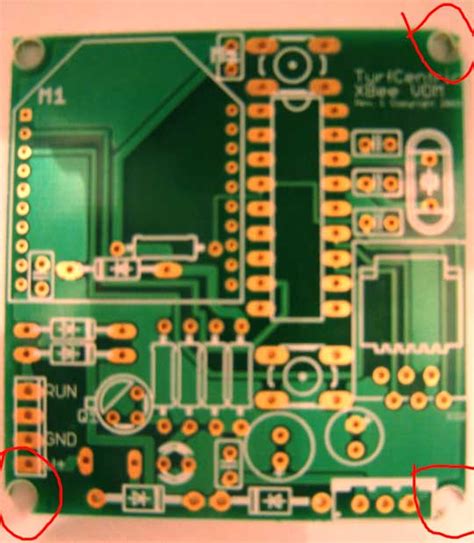
In addition to their electrical functions, drilled holes can also provide mechanical support for the PCB. Mounting holes, for example, are used to attach the PCB to the device chassis or other structural components. These holes are typically larger than those used for component mounting and are strategically placed to ensure proper alignment and stability.
Thermal Management
Drilled holes can also contribute to the thermal management of the PCB. Thermal vias, which are typically filled with a thermally conductive material, are used to transfer heat away from high-power components and distribute it across the board or to an external heatsink. This helps to prevent overheating and ensures the reliable operation of the device.

Design Considerations for PCB Drilled Holes
When designing a PCB, there are several key considerations to keep in mind regarding drilled holes. By addressing these factors early in the design process, you can avoid potential issues and ensure the successful manufacture and operation of your PCB.
Hole Size and Tolerance
One of the most critical aspects of drilled hole design is choosing the appropriate hole size and tolerance. The hole size must be large enough to accommodate the component leads or provide the necessary electrical connections while maintaining sufficient clearance for reliable soldering. Tolerance refers to the acceptable variation in hole size and position, which is important for ensuring proper fit and alignment.
When selecting hole sizes and tolerances, consider the following factors:
– Component lead diameters
– Plating thickness
– Drilling capabilities of the PCB manufacturer
– Soldering requirements
– PCB Thickness
| Hole Type | Typical Size Range | Tolerance |
|---|---|---|
| Through Hole | 0.5mm – 1.0mm | ±0.1mm |
| Blind Via | 0.2mm – 0.5mm | ±0.05mm |
| Buried Via | 0.2mm – 0.5mm | ±0.05mm |
| Micro Via | 0.1mm – 0.15mm | ±0.025mm |
Pad Size and Shape
The pad size and shape around drilled holes are also important considerations. Pads provide a surface for soldering and ensure a reliable connection between the component and the PCB. The pad size should be large enough to accommodate the component lead and allow for proper soldering, while not being so large as to waste space or create unnecessary capacitance.
Pad shapes can vary depending on the application and the type of component being used. Common pad shapes include circular, oval, and rectangular. In some cases, specialized pad shapes may be used to improve soldering or to accommodate unique component geometries.
Hole Placement and Spacing
The placement and spacing of drilled holes on the PCB are critical for ensuring proper functionality and manufacturability. When placing holes, consider the following factors:
- Component footprints and package sizes
- PCB layout and routing requirements
- Manufacturing constraints, such as minimum hole spacing and edge clearance
- Assembly and soldering processes
Proper hole placement and spacing help to avoid issues such as signal interference, manufacturing defects, and assembly difficulties.
Layer Stack-up and Via Design
In multi-layer PCBs, the layer stack-up and via design play a crucial role in the overall performance and reliability of the board. The layer stack-up defines the arrangement of copper layers, insulating layers, and drilled holes, while via design determines how signals are routed between layers.
When designing the layer stack-up and vias, consider the following factors:
– Signal integrity requirements
– Impedance control
– Power distribution
– Manufacturing capabilities and constraints
Proper layer stack-up and via design help to ensure optimal signal quality, minimize crosstalk and EMI, and facilitate efficient power distribution throughout the PCB.

Manufacturing Processes for PCB Drilled Holes
The creation of drilled holes in PCBs involves several manufacturing processes, each of which contributes to the final quality and reliability of the board. Let’s take a closer look at the key processes involved:
Drilling
The first step in creating drilled holes is the actual drilling process. PCB Manufacturers use specialized drilling machines, such as CNC (Computer Numerical Control) drills or laser drills, to create holes in the board.
CNC drilling is the most common method for creating through holes and larger vias. The process involves using a high-speed, computer-controlled drill bit to create holes in the PCB substrate. CNC drilling offers good accuracy and repeatability, making it suitable for a wide range of hole sizes and tolerances.
Laser drilling, on the other hand, is typically used for creating micro vias and other small, precise holes. This process uses a focused laser beam to vaporize the PCB substrate material, creating the desired hole. Laser drilling offers higher precision and smaller hole sizes compared to CNC drilling, making it ideal for high-density designs.
Deburring and Cleaning
After the drilling process, the PCB undergoes deburring and cleaning to remove any debris or rough edges around the holes. Deburring helps to ensure that the holes are smooth and free of burrs, which can interfere with the plating process and cause reliability issues.
Cleaning the PCB involves removing any dust, drill smear, or other contaminants from the hole walls and surfaces. This is typically done using a combination of mechanical and chemical cleaning methods, such as brushing, high-pressure water jetting, and chemical desmearing.
Plating
Once the holes are drilled and cleaned, they are plated with a conductive material, typically copper, to create the electrical connections between layers and to provide a surface for soldering. The plating process involves several steps:
-
Electroless copper deposition: A thin layer of copper is deposited onto the hole walls and surfaces using an electroless plating process. This layer serves as a conductive seed layer for the subsequent electrolytic plating.
-
Electrolytic copper plating: The PCB is immersed in an electrolytic plating bath, where a thicker layer of copper is deposited onto the seed layer. This layer provides the bulk of the electrical conductivity and ensures a strong connection between layers.
-
Finish plating: Depending on the application and requirements, the plated holes may receive an additional finish layer, such as tin, gold, or silver. These finishes provide improved solderability, corrosion resistance, or other desirable properties.
Inspection and Testing
After the plating process, the PCB undergoes a series of inspections and tests to ensure the quality and reliability of the drilled holes. Some common inspection and testing methods include:
- Visual inspection: The PCB is visually inspected for any defects, such as missing or misaligned holes, incomplete plating, or contamination.
-
Automated Optical Inspection (AOI): AOI machines use high-resolution cameras and advanced image processing algorithms to detect and analyze defects in the PCB, including drilled holes.
-
Electrical testing: Various electrical tests, such as continuity testing and insulation resistance testing, are performed to ensure that the drilled holes provide the expected electrical connections and do not exhibit any shorts or opens.
-
Microsectioning: In some cases, a small sample of the PCB may be cross-sectioned and examined under a microscope to assess the quality of the drilled holes and plating.
By conducting thorough inspections and tests, PCB manufacturers can identify and address any issues related to drilled holes, ensuring the overall quality and reliability of the final product.
Common Issues with PCB Drilled Holes
Despite advancements in PCB design and manufacturing processes, there are still several common issues that can arise with drilled holes. Being aware of these issues and taking steps to prevent them can help you avoid surprises and ensure the success of your PCB project.
Misaligned or Missing Holes
One of the most common issues with PCB drilled holes is misalignment or missing holes. This can occur due to various factors, such as:
- Incorrect drill file generation
- Malfunctions in the drilling equipment
- Human error during the setup or operation of the drilling machine
Misaligned or missing holes can lead to component fitment issues, incorrect electrical connections, and overall functional failures of the PCB. To prevent these issues, it is essential to carefully review drill files, use reliable drilling equipment, and implement strict quality control measures during the manufacturing process.
Incomplete or Excessive Plating
Another common issue with PCB drilled holes is incomplete or excessive plating. Incomplete plating occurs when the hole walls are not entirely covered with the conductive material, leading to poor electrical connections and potential reliability issues. Excessive plating, on the other hand, can cause the holes to become too narrow, making it difficult to insert components or leading to stress on the PCB substrate.
To avoid plating issues, it is important to carefully control the plating process parameters, such as the plating time, current density, and solution composition. Regular maintenance and calibration of the plating equipment, as well as thorough inspections and tests, can help to identify and correct any plating issues.
Drill Smear and Contamination
Drill smear and contamination are other common issues that can affect the quality and reliability of PCB drilled holes. Drill smear occurs when the drilling process generates heat and pressure, causing the PCB substrate material to melt and spread across the hole walls. This can lead to poor plating adhesion and electrical connectivity issues.
Contamination can occur when debris, such as dust or oil, accumulates on the hole walls or surfaces during the manufacturing process. This contamination can interfere with the plating process and cause defects in the final product.
To minimize drill smear and contamination, PCB manufacturers use specialized cleaning processes, such as plasma etching or chemical desmearing, to remove any smear or debris from the holes. Proper maintenance of the drilling and plating equipment, as well as the use of clean room environments, can also help to reduce the risk of contamination.
Thermal Stress and Cracking
Thermal stress and cracking are issues that can arise during the soldering process or during the operation of the PCB in high-temperature environments. When the PCB is exposed to high temperatures, the different materials in the board, such as the substrate, copper plating, and solder, can expand and contract at different rates. This can lead to stress on the drilled holes and, in some cases, cause cracking or delamination.
To minimize the risk of thermal stress and cracking, it is important to consider the thermal properties of the materials used in the PCB and to design the board with adequate thermal management features, such as thermal vias or heatsinks. Proper control of the soldering process, including temperature profiles and cooling rates, can also help to reduce thermal stress on the drilled holes.
FAQ
1. What is the difference between through holes and vias?
Through holes are drilled holes that extend completely through the PCB, from one side to the other. They are typically used for mounting through-hole components and providing electrical connections between layers. Vias, on the other hand, are drilled holes that are used specifically for creating electrical connections between layers. They can be blind (starting from one side and terminating at an inner layer), buried (connecting inner layers only), or through (extending through the entire board).
2. What factors should I consider when selecting hole sizes for my PCB?
When selecting hole sizes for your PCB, consider the following factors:
- Component lead diameters: Ensure that the hole size is large enough to accommodate the leads of the components you plan to use.
- Plating thickness: Take into account the thickness of the plating that will be applied to the hole walls, as this will reduce the effective hole diameter.
- Drilling capabilities: Consult with your PCB manufacturer to understand their drilling capabilities and any constraints on hole sizes and tolerances.
- Soldering requirements: Consider the soldering process and ensure that the hole size allows for adequate solder fill and a reliable connection.
- PCB thickness: Thicker PCBs may require larger hole sizes to maintain aspect ratios and ensure reliable plating.
3. What is drill smear, and how can it be prevented?
Drill smear is a common issue that occurs when the drilling process generates heat and pressure, causing the PCB substrate material to melt and spread across the hole walls. This can lead to poor plating adhesion and electrical connectivity issues.
To prevent drill smear, PCB manufacturers use specialized cleaning processes, such as plasma etching or chemical desmearing, to remove any smear from the holes. Additionally, proper control of the drilling process parameters, such as feed rates and drill bit geometry, can help to minimize the generation of heat and pressure that leads to drill smear.
4. How do I ensure proper alignment of drilled holes in my PCB?
To ensure proper alignment of drilled holes in your PCB, consider the following steps:
- Use a consistent and accurate CAD tool for designing your PCB and generating the drill files.
- Clearly communicate your requirements and specifications to your PCB manufacturer, including any critical dimensions or tolerances.
- Request a drill drawing or drill map from your manufacturer to review and approve before production begins.
- Implement a robust quality control process, including visual inspections and automated optical inspection (AOI), to detect any misalignment issues early in the manufacturing process.
- Work with a reputable PCB manufacturer that has a proven track record of producing high-quality boards with accurate hole alignment.
5. What are the benefits of using micro vias in high-density PCB designs?
Micro vias offer several benefits in high-density PCB designs:
- Space savings: Micro vias have smaller diameters than traditional through holes or vias, allowing for more efficient use of board space and enabling higher component densities.
- Improved signal integrity: The smaller size of micro vias reduces the capacitance and inductance associated with the connections, leading to improved signal integrity and reduced crosstalk.
- Increased design flexibility: Micro vias enable more complex routing strategies and allow for the creation of fine-pitch interconnects, supporting advanced packaging technologies and high-speed designs.
- Enhanced reliability: When properly designed and manufactured, micro vias provide reliable electrical connections and can withstand the thermal and mechanical stresses associated with high-density PCB assemblies.
- Cost-effectiveness: Although the manufacturing process for micro vias may be more complex, their use can lead to overall cost savings by enabling smaller board sizes, reducing layer counts, and improving yields.
Conclusion
Drilled holes are a critical aspect of PCB design and manufacturing, serving various functions such as component mounting, electrical connections, mechanical support, and thermal management. By understanding the different types of drilled holes, their design considerations, manufacturing processes, and common issues, you can create PCBs that are reliable, efficient, and cost-effective.
When designing your PCB, pay close attention to hole sizes, tolerances, pad sizes, and placement to ensure proper functionality and manufacturability


Leave a Reply