Introduction to PCB History
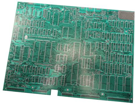
Printed Circuit Boards (PCBs) have revolutionized the electronics industry since their inception in the early 20th century. These boards, which consist of conductive tracks, pads, and other features etched from copper sheets laminated onto a non-conductive substrate, have become an integral part of modern electronic devices. From smartphones and computers to medical equipment and aerospace technology, PCBs are found in virtually every electronic device we use today. In this article, we will delve into the fascinating history of PCBs, tracing their evolution from simple wire-wrapped circuits to the complex, multi-layered boards we use today.
The Early Days of PCB Development
The Invention of the PCB
The concept of the printed circuit board can be traced back to the early 1900s when German inventor Albert Hanson filed a patent for a “printed wire” system in 1903. However, it wasn’t until the 1920s that the first practical PCBs were developed. In 1925, Charles Ducas of the United States filed a patent for a method of creating an electrical path directly on an insulated surface by printing through a stencil with electrically conductive inks. This laid the groundwork for the development of modern PCBs.
The Rise of Wire-Wrapped Circuits
Before the widespread adoption of PCBs, electronic circuits were typically constructed using wire-wrapped connections. This method involved wrapping wires around terminal posts to create the desired electrical connections. While wire-wrapping allowed for the creation of complex circuits, it was a time-consuming and error-prone process. As electronic devices became more sophisticated, the limitations of wire-wrapped circuits became increasingly apparent.
The Development of Modern PCBs
The Introduction of Etched PCBs
In the 1940s, the development of etched PCBs began to gain traction. This process involved etching away unwanted copper from a substrate to create the desired electrical connections. One of the earliest examples of an etched PCB was the “printed wire” board developed by Austrian engineer Paul Eisler in 1943. Eisler’s design was used in the proximity fuse of anti-aircraft shells during World War II, demonstrating the potential of PCBs in military applications.
The Advent of Through-Hole Technology
As PCBs became more widely used, the need for a reliable method of attaching components to the board became apparent. In the 1950s, through-hole technology emerged as the standard for component mounting. This method involved drilling holes in the PCB and inserting component leads through the holes, which were then soldered to the copper tracks on the opposite side of the board. Through-hole technology allowed for the creation of more complex circuits and improved the reliability of electronic devices.
The Rise of Surface-Mount Technology
While through-hole technology was a significant improvement over wire-wrapped circuits, it had its limitations. As electronic devices became smaller and more complex, the need for a more compact and efficient method of component mounting arose. In the 1960s, surface-mount technology (SMT) began to gain popularity. SMT involves placing components directly on the surface of the PCB and soldering them to the copper tracks using a reflow soldering process. This method allows for the creation of smaller, more densely packed circuits, which has been crucial to the development of modern electronic devices.

The Evolution of PCB Materials and Manufacturing Processes
The Transition from Phenolic to Epoxy Resin Substrates
Early PCBs were typically made using phenolic resin substrates, which were inexpensive and easy to work with. However, phenolic resin had its drawbacks, including poor heat resistance and a tendency to absorb moisture. In the 1960s, epoxy resin substrates began to replace phenolic resin as the material of choice for PCBs. Epoxy resin offered improved heat resistance, better electrical insulation, and greater durability, making it better suited for use in high-performance electronic devices.
The Development of Multi-Layer PCBs
As electronic circuits became more complex, the need for PCBs with greater circuit density arose. In the 1960s, the development of multi-layer PCBs began to address this need. Multi-layer PCBs consist of multiple layers of copper tracks separated by insulating layers, allowing for the creation of more complex circuits in a smaller space. The introduction of multi-layer PCBs revolutionized the electronics industry, enabling the development of more sophisticated and compact devices.
| Decade | PCB Development Milestones |
|---|---|
| 1900s | Concept of printed wire system patented by Albert Hanson |
| 1920s | First practical PCBs developed using conductive inks |
| 1940s | Etched PCBs gain traction, used in military applications |
| 1950s | Through-hole technology emerges as standard for component mounting |
| 1960s | Surface-mount technology gains popularity, epoxy resin substrates replace phenolic resin, multi-layer PCBs developed |
Advancements in PCB Manufacturing Processes
As PCBs have evolved, so too have the manufacturing processes used to create them. In the early days of PCB Production, the process was largely manual, with workers hand-placing components and soldering connections. However, as demand for PCBs grew, automated manufacturing processes were developed to improve efficiency and accuracy. Today, PCB manufacturing is a highly automated process, with computer-controlled machines handling everything from component placement to soldering and inspection.
The Impact of PCBs on Modern Electronics
The Role of PCBs in the Miniaturization of Electronic Devices
One of the most significant impacts of PCBs on modern electronics has been their role in the miniaturization of devices. As PCBs have become smaller and more densely packed, electronic devices have become smaller and more portable. This has led to the development of a wide range of compact, high-performance devices, from smartphones and laptops to Wearable Technology and medical implants.
The Importance of PCBs in the Development of New Technologies
PCBs have also played a crucial role in the development of new technologies. From the early days of radio and television to the rise of the internet and the proliferation of smart devices, PCBs have been at the heart of many of the most significant technological advancements of the past century. As new technologies continue to emerge, PCBs will undoubtedly continue to play a vital role in their development and implementation.
The Future of PCBs
Emerging Trends in PCB Design and Manufacturing
As the demand for smaller, faster, and more powerful electronic devices continues to grow, PCB design and manufacturing processes are evolving to keep pace. One emerging trend is the use of high-density interconnect (HDI) PCBs, which allow for even greater circuit density and miniaturization. Another trend is the increasing use of flexible and rigid-Flex PCBs, which offer greater design flexibility and improved reliability in applications where traditional rigid PCBs may not be suitable.
The Potential Impact of New Materials and Technologies on PCB Development
In addition to advances in design and manufacturing processes, new materials and technologies are also poised to have a significant impact on the future of PCBs. For example, the use of advanced materials such as graphene and carbon nanotubes could lead to the development of PCBs with improved thermal and electrical properties. Additionally, the integration of embedded components and 3D printing technologies could open up new possibilities for PCB design and functionality.
Frequently Asked Questions (FAQ)
-
What is a printed circuit board (PCB)?
A printed circuit board (PCB) is a flat board made of insulating material with conductive tracks, pads, and other features etched from copper sheets laminated onto its surface. It is used to mechanically support and electrically connect electronic components using conductive pathways. -
What are the advantages of using PCBs over wire-wrapped circuits?
PCBs offer several advantages over wire-wrapped circuits, including improved reliability, greater circuit density, and faster assembly times. PCBs also allow for the creation of more complex circuits and are better suited for use in high-volume production. -
What is the difference between through-hole and surface-mount technology?
Through-hole technology involves inserting component leads through holes drilled in the PCB and soldering them to the copper tracks on the opposite side of the board. Surface-mount technology (SMT) involves placing components directly on the surface of the PCB and soldering them to the copper tracks using a reflow soldering process. SMT allows for the creation of smaller, more densely packed circuits compared to through-hole technology. -
What are multi-layer PCBs, and what are their advantages?
Multi-layer PCBs consist of multiple layers of copper tracks separated by insulating layers, allowing for the creation of more complex circuits in a smaller space. The advantages of multi-layer PCBs include greater circuit density, improved signal integrity, and better EMI/RFI shielding compared to single-layer boards. -
How have PCBs contributed to the miniaturization of electronic devices?
As PCBs have become smaller and more densely packed, they have enabled the development of smaller and more portable electronic devices. The use of surface-mount technology and multi-layer PCBs has allowed for the creation of highly compact, high-performance devices, such as smartphones, laptops, and wearable technology.
Conclusion
The history of printed circuit boards is a fascinating story of innovation, ingenuity, and technological advancement. From their humble beginnings as simple wire-wrapped circuits to the complex, multi-layered boards we use today, PCBs have played a crucial role in the development of modern electronics. As we look to the future, it is clear that PCBs will continue to evolve and adapt to meet the ever-changing needs of the electronics industry. With new materials, technologies, and manufacturing processes on the horizon, the possibilities for PCB design and functionality are virtually limitless. As we continue to push the boundaries of what is possible with electronic devices, PCBs will undoubtedly remain at the heart of these advancements, driving innovation and shaping the future of technology.
Leave a Reply