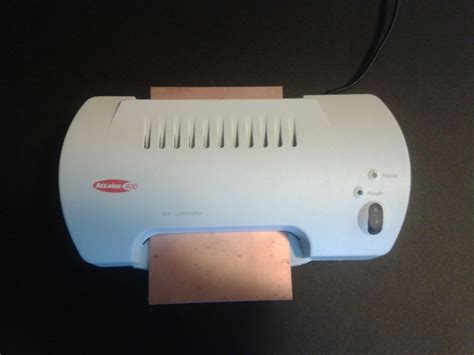
What is PCB Lamination?
PCB lamination is a critical step in the manufacturing of Printed Circuit Boards (PCBs). It involves bonding multiple layers of PCB material together using heat and pressure to create a single, solid board. The lamination process ensures that the conductive copper traces are properly insulated and protected, and that the board has the necessary strength and rigidity to withstand the stresses of assembly and use.
The Importance of PCB Lamination
PCB lamination is essential for several reasons:
- Insulation: Lamination provides insulation between the conductive copper layers, preventing short circuits and ensuring proper electrical functionality.
- Strength: Bonding the layers together creates a strong, rigid board that can withstand the stresses of handling, assembly, and use.
- Durability: Lamination protects the copper traces from damage due to environmental factors such as moisture, chemicals, and physical impact.
- Reliability: A well-laminated PCB is less likely to suffer from delamination, which can cause electrical failures and reduce the board’s lifespan.
The PCB Lamination Process
The PCB lamination process typically involves the following steps:
1. Material Preparation
The first step in PCB lamination is to prepare the materials. This includes:
- Cleaning the Copper Foil to remove any contaminants
- Applying a thin layer of epoxy resin to the foil
- Cutting the dielectric substrate material (such as FR-4) to the appropriate size
- Stacking the layers in the proper order (copper, substrate, copper)
2. Layup
Once the materials are prepared, they are laid up in a stack in the proper sequence. The stack typically includes:
- A bottom layer of copper foil
- Multiple layers of dielectric substrate material
- A top layer of copper foil
- Additional layers of prepreg (pre-impregnated) material between each layer of substrate
The number of layers and the specific materials used will depend on the design of the PCB.
3. Lamination
The layup stack is then placed in a lamination press, which applies heat and pressure to bond the layers together. The lamination process typically involves the following steps:
- The stack is placed between two metal plates in the press.
- The press applies a specific amount of pressure to the stack, typically ranging from 300 to 500 PSI (pounds per square inch).
- The press heats the stack to a specific temperature, typically between 350°F and 375°F (175°C to 190°C).
- The stack is held at this temperature and pressure for a specific amount of time, typically 1 to 2 hours.
- The press then cools the stack back down to room temperature while maintaining pressure.
The specific pressure, temperature, and time used will depend on the materials being laminated and the thickness of the board.
4. Inspection and Testing
After lamination, the PCB is inspected and tested to ensure that it meets the necessary quality standards. This may include:
- Visual inspection for defects such as blisters, delamination, or warping
- Electrical testing to ensure proper connectivity and functionality
- Microsectioning to examine the internal structure of the board
- Thermal stress testing to ensure the board can withstand high temperatures
- Mechanical stress testing to ensure the board can withstand physical stresses
If the board passes inspection and testing, it moves on to the next stage of the manufacturing process, which may include drilling, plating, and finishing.

Factors Affecting PCB Lamination
Several factors can affect the quality and reliability of PCB lamination, including:
1. Material Selection
The choice of materials used in the PCB can have a significant impact on the lamination process and the final quality of the board. Factors to consider include:
- The type of dielectric substrate material (e.g., FR-4, polyimide, ceramic)
- The thickness and weight of the copper foil
- The Glass Transition Temperature (Tg) of the materials
- The coefficient of thermal expansion (CTE) of the materials
Choosing materials with compatible properties and appropriate specifications for the intended application is crucial for successful lamination.
2. Lamination Parameters
The specific parameters used during lamination, such as pressure, temperature, and time, can also affect the quality of the final board. Factors to consider include:
- The recommended lamination parameters for the specific materials being used
- The thickness of the board and the number of layers being laminated
- The size and shape of the board
- The type of lamination press being used
Following the recommended parameters and adjusting them as needed for the specific board design is important for achieving proper lamination.
3. Cleanliness and Contamination
Contamination of the materials or the lamination environment can lead to defects in the final board. Common sources of contamination include:
- Dust, dirt, or other particles on the copper foil or substrate material
- Oils or other residues from handling or processing
- Moisture or humidity in the lamination environment
Proper cleaning and handling procedures, as well as controlling the lamination environment, can help minimize contamination and ensure consistent results.

Common PCB Lamination Defects
Despite careful material selection and process control, defects can still occur during PCB lamination. Some common defects include:
1. Delamination
Delamination occurs when the layers of the PCB separate or fail to bond properly. This can be caused by:
- Incompatible materials or improper material preparation
- Insufficient pressure or temperature during lamination
- Contamination or moisture between the layers
- Thermal or mechanical stress during subsequent processing steps
Delamination can lead to electrical failures and reduce the lifespan of the board.
2. Blistering
Blistering occurs when small bubbles or voids form between the layers of the PCB. This can be caused by:
- Outgassing of moisture or other volatile compounds during lamination
- Insufficient pressure or temperature during lamination
- Contamination or impurities in the materials
Blistering can weaken the board and lead to delamination or other failures.
3. Warping
Warping occurs when the PCB bends or twists out of its intended shape. This can be caused by:
- Uneven heating or cooling during lamination
- Differences in the coefficient of thermal expansion (CTE) between layers
- Excessive pressure during lamination
- Improper handling or storage after lamination
Warping can make the board difficult to assemble or cause stress on components, leading to failures.

Frequently Asked Questions (FAQ)
1. What is the difference between prepreg and core material in PCB lamination?
Prepreg (pre-impregnated) material is a dielectric substrate that is partially cured and contains a resin system. It is used between layers of core material to bond them together during lamination. Core material, on the other hand, is a fully cured dielectric substrate that provides the primary structure of the PCB.
2. Can different types of materials be laminated together in a single PCB?
Yes, different types of materials can be laminated together in a single PCB, such as FR-4 and polyimide. However, it is important to choose materials with compatible properties, such as similar glass transition temperatures (Tg) and coefficients of thermal expansion (CTE), to ensure proper bonding and minimize stress on the board.
3. What is the typical temperature and pressure used in PCB lamination?
The typical temperature used in PCB lamination ranges from 350°F to 375°F (175°C to 190°C), while the typical pressure ranges from 300 to 500 PSI (pounds per square inch). However, the specific parameters used may vary depending on the materials being laminated and the thickness of the board.
4. How can contamination be minimized during PCB lamination?
Contamination can be minimized during PCB lamination by following proper cleaning and handling procedures, such as:
- Cleaning the copper foil and substrate materials before lamination
- Handling materials with gloves to avoid oils and residues from skin contact
- Storing materials in a clean, dry environment
- Controlling the humidity and temperature of the lamination environment
5. What are some common tests performed on PCBs after lamination?
Common tests performed on PCBs after lamination include:
- Visual inspection for defects such as blisters, delamination, or warping
- Electrical testing to ensure proper connectivity and functionality
- Microsectioning to examine the internal structure of the board
- Thermal stress testing to ensure the board can withstand high temperatures
- Mechanical stress testing to ensure the board can withstand physical stresses
These tests help ensure that the PCB meets the necessary quality and reliability standards for its intended application.
Conclusion
PCB lamination is a critical step in the manufacturing of printed circuit boards, providing insulation, strength, and protection for the conductive copper traces. By carefully selecting materials, controlling the lamination process, and inspecting the finished board, manufacturers can ensure that their PCBs meet the necessary quality and reliability standards for their intended applications. While defects can still occur, understanding the factors that affect lamination and the common types of defects can help manufacturers optimize their processes and minimize issues. As PCB technology continues to evolve, the lamination process will remain a key focus for ensuring the performance and longevity of these essential components.


Leave a Reply