Introduction to PCB Carbon Contacts
Carbon contacts are an increasingly popular choice for use on printed circuit boards (PCBs) due to their excellent electrical conductivity, durability, and cost-effectiveness compared to other contact materials like gold or silver. Carbon contacts can be applied to PCBs using various methods such as screen printing, pad printing, or inkjet printing.
Using carbon contacts on PCBs offers several advantages:
- High electrical conductivity
- Excellent wear resistance and durability
- Low contact resistance
- Cost-effective alternative to precious metal contacts
- RoHS compliant and environmentally friendly
In this article, we’ll dive into the process of applying carbon contacts to PCBs, the equipment and materials needed, design considerations, quality control measures, and troubleshooting common issues. By the end, you’ll have a comprehensive understanding of how to successfully implement carbon contacts in your PCB manufacturing process.
PCB Carbon Contact Application Methods
There are several methods available for applying carbon contacts to PCBs, each with its own advantages and considerations. The three most common methods are:
- Screen Printing
- Pad Printing
- Inkjet Printing
Let’s explore each method in more detail.
Screen Printing Carbon Contacts
Screen printing is a popular and versatile method for applying carbon contacts to PCBs. It involves forcing carbon ink through a fine mesh screen onto the PCB surface using a squeegee. The screen has a stencil of the desired contact pattern, allowing the ink to pass through only in the intended areas.
Advantages of screen printing:
– High throughput and efficiency for large-scale production
– Ability to print on various PCB materials and surface finishes
– Good control over ink thickness and consistency
– Cost-effective for high-volume runs
Considerations for screen printing:
– Requires a separate screen for each unique contact pattern
– Higher setup costs compared to other methods
– Limited resolution compared to other printing methods
Pad Printing Carbon Contacts
Pad printing is another option for applying carbon contacts to PCBs, particularly for smaller contact areas or irregular surfaces. This method uses a silicone pad to pick up ink from an etched plate (cliché) and transfer it onto the PCB surface.
Advantages of pad printing:
– Ability to print on irregular or curved PCB surfaces
– Higher resolution and finer detail compared to screen printing
– Lower setup costs compared to screen printing
– Ideal for smaller contact areas or complex patterns
Considerations for pad printing:
– Lower throughput compared to screen printing
– Requires frequent ink refills and pad cleaning for consistent prints
– Limited ink thickness control compared to screen printing
Inkjet Printing Carbon Contacts
Inkjet printing is a digital, non-contact method for applying carbon contacts to PCBs. It uses a print head with multiple nozzles to deposit tiny droplets of carbon ink onto the PCB surface in the desired pattern.
Advantages of inkjet printing:
– High resolution and precision for fine-pitch contacts
– Digital process allows for quick design changes without new screens or plates
– Minimal waste and efficient ink usage
– Ideal for low-volume prototyping or high-mix production
Considerations for inkjet printing:
– Higher equipment costs compared to other methods
– Requires specialized carbon inks with optimized viscosity and particle size
– Slower print speed compared to screen or pad printing
– Potential for nozzle clogging and print head maintenance

Equipment and Materials for PCB Carbon Contact Application
To apply carbon contacts to PCBs, you’ll need the following equipment and materials based on your chosen application method:
Screen Printing Equipment and Materials
- Screen printing machine
- Printing screens with contact pattern stencils
- Squeegees
- Carbon ink suitable for screen printing
- Drying/curing oven or UV curing system
Pad Printing Equipment and Materials
- Pad printing machine
- Etched plates (clichés) with contact patterns
- Silicone pads
- Carbon ink suitable for pad printing
- Drying/curing oven or UV curing system
Inkjet Printing Equipment and Materials
- Inkjet printer with print head and control software
- Carbon ink optimized for inkjet printing
- Substrate handling and positioning system
- Drying/curing oven or UV curing system
In addition to the printing equipment, you’ll also need:
- PCB substrates (FR-4, polyimide, etc.)
- Pre-treatment chemicals for PCB surface preparation
- Cleaning solvents and wipes for equipment maintenance
- Personal protective equipment (gloves, goggles, etc.)
It’s crucial to select high-quality carbon inks that are compatible with your chosen printing method and PCB substrate material. Work with reputable suppliers and conduct thorough testing to ensure optimal print quality and electrical performance.

PCB Design Considerations for Carbon Contacts
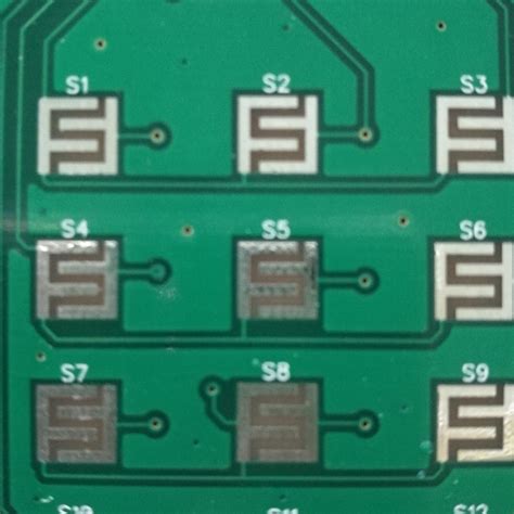
When designing PCBs with carbon contacts, there are several key considerations to keep in mind to ensure optimal functionality and manufacturability:
Contact Size and Spacing
- Determine the minimum contact size based on the printing method and carbon ink properties
- Maintain adequate spacing between contacts to prevent bridging or short circuits
- Consider the aspect ratio of contact width to ink thickness for proper printing and adhesion
Soldermask and Legend Placement
- Ensure soldermask openings are slightly larger than the contact area to prevent ink bleeding
- Keep legend markings away from contact areas to avoid interference with printing or electrical contact
Pad Shape and Layout
- Use simple, symmetrical pad shapes for easier printing and consistent contact area
- Avoid acute angles or narrow necks that may cause ink pooling or uneven distribution
- Optimize pad layout for efficient printing and minimized ink usage
Surface Finish Compatibility
- Select a PCB Surface Finish that is compatible with carbon ink adhesion (e.g., ENIG, OSP)
- Avoid highly reflective or smooth finishes that may hinder ink wetting or adhesion
- Consider any special surface preparation requirements for the chosen finish and ink
By carefully considering these design factors and collaborating closely with your PCB manufacturer and carbon ink supplier, you can create PCB designs that are optimized for carbon contact printing and ensure high-quality, reliable results.

Quality Control for PCB Carbon Contacts
Implementing a robust quality control process is essential to ensure consistent, high-performance carbon contacts on your PCBs. Key quality control measures include:
Visual Inspection
- Check for any missing, incomplete, or deformed contacts
- Look for signs of ink smearing, bridging, or contamination
- Verify proper alignment and registration of contacts to pads
Electrical Testing
- Measure contact resistance using a 4-wire Kelvin probe or similar method
- Perform continuity and isolation testing to detect any short circuits or open connections
- Conduct environmental testing (e.g., temperature cycling, humidity exposure) to assess contact durability
Adhesion Testing
- Perform tape test or scratch test to evaluate ink adhesion to PCB surface
- Assess contact durability under mechanical stress or abrasion
- Verify compatibility with downstream processes (e.g., soldering, encapsulation)
Statistical Process Control (SPC)
- Monitor key process parameters (e.g., ink viscosity, print speed, curing temperature) for consistency
- Use control charts to track contact resistance and other critical quality attributes over time
- Implement corrective actions and process improvements based on SPC data analysis
| Quality Control Measure | Frequency | Acceptance Criteria |
|---|---|---|
| Visual Inspection | 100% | No visible defects |
| Contact Resistance | Sampling | < 100 mΩ |
| Continuity/Isolation | Sampling | 100% pass |
| Ink Adhesion | Sampling | 4B minimum |
By implementing a comprehensive quality control plan and regularly monitoring process performance, you can identify and address any issues early on, ensuring consistent, high-quality carbon contacts on your PCBs.
Troubleshooting Common Issues with PCB Carbon Contacts
Even with careful design and process control, issues can sometimes arise when applying carbon contacts to PCBs. Here are some common problems and potential solutions:
Incomplete or Missing Contacts
- Check screen or plate for any blockages or damage
- Verify proper ink viscosity and printing parameters
- Ensure adequate ink volume in screen or pad
Ink Smearing or Bridging
- Adjust squeegee pressure and speed for screen printing
- Optimize pad hardness and pressure for pad printing
- Verify proper ink viscosity and drying/curing conditions
Poor Ink Adhesion
- Ensure PCB surface is clean and free of contaminants
- Verify compatibility of ink with PCB surface finish
- Optimize curing temperature and time for better adhesion
High Contact Resistance
- Check for any contaminants or oxidation on contact surface
- Verify proper ink formulation and particle size distribution
- Ensure complete ink curing and avoid any voids or thin spots
Inconsistent Print Quality
- Monitor and control environmental conditions (temperature, humidity)
- Perform regular equipment maintenance and calibration
- Implement SPC to identify and correct any process drift
By quickly identifying and addressing these issues, you can minimize downtime, improve yield, and ensure high-quality carbon contacts on your PCBs.
Frequently Asked Questions (FAQ)
1. What are the advantages of using carbon contacts on PCBs?
Carbon contacts offer several advantages over other materials like gold or silver, including:
- High electrical conductivity
- Excellent durability and wear resistance
- Low contact resistance
- Cost-effectiveness
- RoHS compliance and environmental friendliness
2. What methods can be used to apply carbon contacts to PCBs?
The three most common methods for applying carbon contacts to PCBs are:
- Screen Printing: Forcing ink through a fine mesh screen onto the PCB surface
- Pad Printing: Using a silicone pad to transfer ink from an etched plate to the PCB
- Inkjet Printing: Depositing ink droplets onto the PCB using a digital print head
Each method has its own advantages and considerations based on factors like contact size, surface irregularity, resolution, and production volume.
3. What should I consider when designing PCBs with carbon contacts?
Key design considerations for PCBs with carbon contacts include:
- Contact size and spacing
- Soldermask and legend placement
- Pad shape and layout
- Surface finish compatibility
Work closely with your PCB manufacturer and carbon ink supplier to optimize your design for printability and performance.
4. How can I ensure consistent, high-quality carbon contacts on my PCBs?
Implement a robust quality control plan that includes:
- Visual inspection for defects and irregularities
- Electrical testing for contact resistance, continuity, and isolation
- Adhesion testing to verify ink-to-PCB bonding
- Statistical process control (SPC) to monitor and optimize critical process parameters
Regularly review quality data and implement continuous improvement initiatives to maintain high standards.
5. What are some common issues with carbon contacts and how can I troubleshoot them?
Common issues with PCB carbon contacts include:
- Incomplete or missing contacts
- Ink smearing or bridging
- Poor ink adhesion
- High contact resistance
- Inconsistent print quality
Troubleshoot these issues by:
- Checking screens, plates, and equipment for damage or blockages
- Verifying ink viscosity, printing parameters, and curing conditions
- Ensuring PCB surface cleanliness and compatibility
- Monitoring environmental conditions and conducting regular maintenance
- Implementing SPC to identify and correct process drift
By promptly addressing these issues, you can minimize their impact on PCB Quality and production efficiency.
Conclusion
Applying carbon contacts to PCBs offers numerous benefits, including high conductivity, durability, and cost-effectiveness. By understanding the various application methods, design considerations, quality control measures, and troubleshooting techniques, you can successfully implement carbon contacts in your PCB manufacturing process.
Remember to work closely with your suppliers, optimize your designs for printability, and continuously monitor and improve your processes to ensure the highest quality results. With the right approach and expertise, carbon contacts can provide a reliable and high-performance solution for your PCB needs.


Leave a Reply