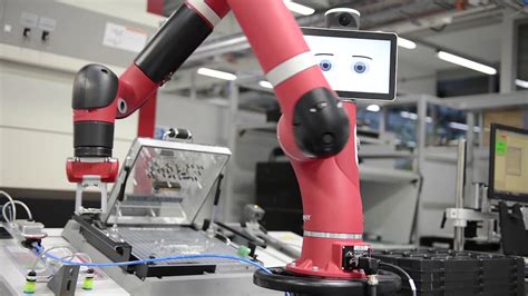
What are PCBs and Why are They Essential in Robotics?
PCBs are thin boards made of insulating materials, such as fiberglass or plastic, with conductive copper tracks etched onto their surface. These tracks form the electrical connections between various components mounted on the board, such as microcontrollers, sensors, and power regulators. PCBs provide a compact and efficient way to organize and route the complex circuitry required in robots.
In robotics, PCBs serve several critical functions:
- Interconnectivity: PCBs allow for the interconnection of various electronic components, enabling communication and power distribution among them.
- Miniaturization: By consolidating circuitry onto a single board, PCBs enable the creation of compact and lightweight robots.
- Reliability: Well-designed PCBs ensure stable and reliable electrical connections, reducing the risk of failures and malfunctions.
- Customization: PCBs can be customized to meet the specific requirements of a robot, accommodating unique sensor configurations, actuator interfaces, and communication protocols.
PCB Design Considerations for Robots
Designing PCBs for robots involves several key considerations to ensure optimal performance, reliability, and functionality. Some of these considerations include:
Component Selection and Placement
Choosing the right components is crucial for the success of a robot’s PCB. Factors such as power requirements, operating conditions, and compatibility with other components must be carefully evaluated. Additionally, the placement of components on the board should be optimized for signal integrity, thermal management, and mechanical stability.
Signal Integrity and EMI Mitigation
Robots often operate in environments with potential electromagnetic interference (EMI) sources, such as motors and wireless communication devices. Ensuring signal integrity and minimizing EMI is essential to maintain reliable operation. Techniques such as proper grounding, shielding, and the use of differential signaling can help mitigate EMI issues.
Power Management
Efficient power management is critical in robotics, as robots often rely on batteries or have limited power budgets. PCB designers must incorporate power regulation circuitry, such as Voltage Regulators and power monitors, to ensure stable and efficient power delivery to all components. Techniques like power sequencing and load sharing can further optimize power usage.
Thermal Management
Robots generate heat during operation, which can affect the performance and lifespan of electronic components. Effective thermal management is necessary to dissipate heat and maintain optimal operating temperatures. PCB designers can employ techniques such as thermal vias, heat sinks, and strategic component placement to enhance heat dissipation.
Mechanical Considerations
PCBs in robots must withstand various mechanical stresses, such as vibrations, shocks, and physical impacts. Designers must consider the mechanical stability of the PCB, including the choice of board materials, thickness, and mounting methods. Reinforced PCBs, Conformal Coatings, and shock-absorbing mounting solutions can enhance the mechanical resilience of the board.

PCB Manufacturing Process for Robots
The manufacturing process for PCBs used in robots involves several steps to ensure high quality and reliability. Here’s an overview of the typical PCB manufacturing process:
- Design and Layout: The PCB design is created using specialized software, such as EDA (Electronic Design Automation) tools. The layout includes the placement of components, routing of tracks, and the creation of solder masks and silkscreen layers.
- Prototyping: Before mass production, prototypes of the PCB are often fabricated for testing and validation. Prototyping allows for the identification and correction of any design issues or performance concerns.
- Fabrication: The PCB Fabrication process begins with the creation of a copper-clad laminate board. The copper layer is then patterned using photolithography and etching techniques to form the conductive tracks and pads.
- Drilling: Holes are drilled through the board to accommodate through-hole components and provide electrical connections between layers.
- Plating: The drilled holes are plated with copper to establish electrical continuity between layers.
- Solder Mask and Silkscreen: A solder mask layer is applied to the board to protect the copper tracks from accidental shorts and provide insulation. The silkscreen layer is then added to label components and provide visual references.
- Surface Finishing: A surface finish, such as HASL (Hot Air Solder Leveling) or ENIG (Electroless Nickel Immersion Gold), is applied to the exposed copper pads to prevent oxidation and enhance solderability.
- Electrical Testing: The manufactured PCBs undergo thorough electrical testing to ensure continuity, isolation, and functionality.
- Assembly: The PCB is populated with components using automated pick-and-place machines or manual soldering techniques. The assembled board is then inspected for quality and functionality.
| Step | Description |
|---|---|
| Design and Layout | Creation of PCB design using EDA software |
| Prototyping | Fabrication of Prototype Boards for testing |
| Fabrication | Patterning of copper traces on the laminate board |
| Drilling | Creation of holes for through-hole components and interlayer connections |
| Plating | Copper plating of drilled holes for electrical continuity |
| Solder Mask and Silkscreen | Application of protective solder mask and informative silkscreen layers |
| Surface Finishing | Application of surface finish to exposed copper pads |
| Electrical Testing | Thorough testing of PCB functionality and connectivity |
| Assembly | Population of components on the PCB and final inspection |

Future Trends in PCB Design for Robotics
The field of robotics is constantly evolving, and PCB design plays a crucial role in enabling new capabilities and innovations. Here are some future trends shaping the PCB design landscape in robotics:
Miniaturization and High-Density Packaging
As robots become more compact and sophisticated, there is a growing demand for miniaturized PCBs with high-density component packaging. Advanced packaging technologies, such as System-in-Package (SiP) and 3D packaging, allow for the integration of multiple components into a single package, reducing board size and improving performance.
Flexible and Stretchable PCBs
Flexible and stretchable PCBs are gaining traction in robotics, particularly in wearable and soft robotics applications. These PCBs can conform to complex shapes and withstand mechanical deformations, enabling the integration of electronics into flexible and bendable structures.
Wireless Connectivity and IoT Integration
The integration of wireless connectivity and Internet of Things (IoT) capabilities is becoming increasingly prevalent in robotics. PCBs designed for robots often incorporate wireless modules, such as Wi-Fi, Bluetooth, or cellular, to enable remote control, data transmission, and cloud connectivity.
Advanced Sensors and Actuators
Robots rely on a wide range of sensors and actuators to perceive and interact with their environment. PCB designs are evolving to accommodate advanced sensors, such as MEMS (Micro-Electro-Mechanical Systems) sensors, high-resolution cameras, and 3D sensing modules. Additionally, PCBs are being optimized for driving and controlling various actuators, including motors, servos, and piezoelectric elements.
Artificial Intelligence and Edge Computing
The integration of artificial intelligence (AI) and edge computing capabilities into robots is driving new requirements for PCB design. PCBs are being designed to accommodate powerful processors, such as GPUs and AI accelerators, to enable on-board data processing and decision-making. Edge computing allows robots to process data locally, reducing latency and improving responsiveness.

Frequently Asked Questions (FAQ)
-
What are the benefits of using PCBs in robots compared to other wiring methods?
PCBs offer several benefits over other wiring methods, such as Breadboards or point-to-point wiring. PCBs provide a compact and organized way to route electrical connections, reducing wiring complexity and improving reliability. They also enable the integration of multiple components onto a single board, saving space and simplifying assembly. -
How do I choose the right components for a robot’s PCB?
Choosing the right components for a robot’s PCB involves considering factors such as power requirements, operating conditions, and compatibility with other components. It’s important to select components that meet the specific needs of the robot, such as sensors with the required sensitivity, actuators with sufficient torque, and microcontrollers with the necessary processing power. Consulting datasheets, application notes, and seeking expert advice can help in making informed component choices. -
What are some common challenges in designing PCBs for robots?
Designing PCBs for robots comes with several challenges. Signal integrity and EMI mitigation are critical concerns, as robots often operate in environments with potential electromagnetic interference sources. Ensuring proper power management and thermal management is also crucial to maintain stable and reliable operation. Additionally, mechanical considerations, such as vibration and shock resistance, must be addressed to ensure the PCB can withstand the rigors of robotic applications. -
How can I ensure the reliability and durability of PCBs in robots?
To ensure the reliability and durability of PCBs in robots, several strategies can be employed. Using high-quality components and materials, such as industrial-grade PCBs and connectors, can enhance the board’s resilience. Implementing robust design practices, such as proper grounding, shielding, and strain relief, can mitigate potential failure points. Thorough testing and validation, including environmental and stress testing, can help identify and address any weaknesses in the PCB design. -
What are some emerging technologies in PCB design for robotics?
Emerging technologies in PCB design for robotics include flexible and stretchable PCBs, which enable the integration of electronics into flexible and bendable structures. Advanced packaging technologies, such as System-in-Package (SiP) and 3D packaging, are being used to miniaturize PCBs and improve performance. The integration of wireless connectivity, IoT capabilities, and artificial intelligence is also driving new requirements for PCB design in robotics.
Conclusion
PCBs are the unsung heroes in the world of robotics, providing the essential electrical infrastructure that brings robots to life. From enabling interconnectivity and miniaturization to ensuring reliability and customization, PCBs play a critical role in the functionality and performance of robots. Designing PCBs for robots involves careful consideration of component selection, signal integrity, power management, thermal management, and mechanical stability.
As the field of robotics continues to evolve, PCB design is keeping pace with new trends and technologies. Miniaturization, high-density packaging, flexible and stretchable PCBs, wireless connectivity, advanced sensors and actuators, and the integration of artificial intelligence are shaping the future of PCB design in robotics.
By understanding the importance of PCBs in robots, their design considerations, manufacturing processes, and future trends, designers and engineers can create robust and innovative robotic systems that push the boundaries of what is possible. As robots become increasingly prevalent in various industries and applications, the role of PCBs will only continue to grow in importance, driving the advancement of robotics technology.


Leave a Reply