Introduction to PCB Stencils
PCB stencils are an essential tool in the process of printed Circuit board assembly. They allow for precise and efficient application of solder paste onto the PCB pads, ensuring a high-quality and reliable solder joint. In this article, we will delve into the world of advanced PCB and stencil services, exploring the various aspects of PCB stencil design, fabrication, and usage.
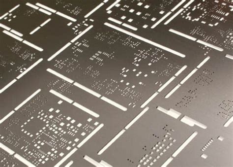
What are PCB Stencils?
PCB stencils, also known as solder paste stencils, are thin metal sheets with apertures that correspond to the solder pads on a printed circuit board. They are used to apply solder paste onto the PCB pads before component placement and reflow soldering. The stencil ensures that the correct amount of solder paste is deposited on each pad, resulting in a consistent and reliable solder joint.
Why are PCB Stencils Important?
PCB stencils play a crucial role in the surface mount technology (SMT) assembly process. They offer several benefits, including:
- Precision: Stencils allow for precise control over the amount and placement of solder paste on the PCB pads, ensuring consistent solder joints.
- Efficiency: Using stencils significantly speeds up the solder paste application process compared to manual methods, making it suitable for high-volume production.
- Repeatability: Stencils ensure that the solder paste application process is repeatable, reducing variations and improving overall quality.
- Cost-effectiveness: By reducing solder paste waste and minimizing rework due to soldering defects, stencils contribute to cost savings in the PCB Assembly process.
PCB Stencil Design Considerations
Designing a PCB stencil involves several key considerations to ensure optimal performance and reliability. Let’s explore some of these factors:
Aperture Size and Shape
The aperture size and shape on the stencil should match the corresponding solder pads on the PCB. The aperture dimensions are typically slightly larger than the pad size to allow for proper solder paste release. The most common aperture shapes are rectangular and circular, depending on the pad geometry.
Stencil Thickness
The thickness of the stencil determines the amount of solder paste deposited on the pads. The optimal stencil thickness depends on various factors, such as the component pitch, pad size, and solder paste properties. Common stencil thicknesses range from 0.1mm to 0.2mm (4-8 mils).
Aperture Wall Angle
The aperture wall angle, also known as the sidewall angle, affects the release of solder paste from the stencil. A typical wall angle is between 45° and 60° to facilitate smooth paste release and prevent clogging.
Stencil Material
Stencils are typically made from stainless steel due to its durability, stability, and resistance to wear. Other materials, such as nickel-plated stainless steel or laser-cut polyimide, are also used in certain applications.
Fiducial Marks
Fiducial marks are reference points on the stencil that align with corresponding marks on the PCB. They ensure proper alignment between the stencil and the PCB during the solder paste printing process.

PCB Stencil Fabrication Methods
There are several methods for fabricating PCB stencils, each with its own advantages and limitations. Let’s explore the most common fabrication techniques:
Laser Cutting
Laser cutting is a popular method for PCB stencil fabrication. It involves using a high-powered laser to cut the apertures in the stencil material. Laser cutting offers several advantages, including:
- High precision and accuracy
- Quick turnaround times
- Ability to create intricate aperture shapes
- Suitable for prototype and low-volume production
However, laser cutting may have limitations in terms of minimum aperture size and wall angle control.
Chemical Etching
Chemical etching is another common method for PCB stencil fabrication. It involves selectively removing material from the stencil sheet using a chemical etchant. The process steps include:
- Applying a photoresist layer to the stencil material
- Exposing the photoresist to UV light through a photomask with the desired aperture pattern
- Developing the photoresist to remove the exposed areas
- Etching the stencil material using a chemical etchant
- Stripping the remaining photoresist
Chemical etching offers good dimensional accuracy and can produce fine apertures. However, it may have limitations in terms of aperture wall angle control and can be more time-consuming compared to laser cutting.
Electroforming
Electroforming is a specialized PCB stencil fabrication method that involves electroplating metal onto a master pattern to create the stencil. The process steps include:
- Creating a master pattern with the desired aperture layout
- Electroplating a layer of metal (typically nickel) onto the master pattern
- Removing the electroformed metal layer from the master pattern
- Mounting the electroformed stencil onto a frame
Electroforming offers several advantages, such as the ability to create very fine apertures and precise wall angle control. However, it is typically more expensive and time-consuming compared to laser cutting and chemical etching.

Stencil Printing Process
The stencil printing process is a critical step in PCB assembly where solder paste is applied onto the PCB pads using the stencil. Let’s overview the key steps involved:
Stencil Alignment
The first step is to align the stencil with the PCB using the fiducial marks. Proper alignment ensures that the solder paste is deposited accurately on the pads.
Solder Paste Application
Once the stencil is aligned, solder paste is applied onto the stencil surface. A squeegee blade is then used to spread the solder paste across the stencil, forcing it through the apertures and onto the PCB pads.
Stencil Cleaning
After the solder paste is applied, the stencil is removed from the PCB. It is important to clean the stencil regularly to prevent solder paste buildup and ensure consistent printing quality.
Inspection
After the stencil printing process, the PCB is inspected to verify the proper solder paste deposition. Automated inspection systems, such as solder paste inspection (SPI) machines, are often used to detect any printing defects.

Stencil Maintenance and Storage
Proper maintenance and storage of PCB stencils are essential to ensure their longevity and consistent performance. Here are some key considerations:
Cleaning
Regular cleaning of the stencil is necessary to remove solder paste residue and prevent clogging of the apertures. Stencils can be cleaned using specialized cleaning agents and equipment, such as stencil cleaning machines or ultrasonic cleaners.
Inspection
Stencils should be periodically inspected for any signs of wear, damage, or contamination. Common issues include bent or warped stencils, damaged apertures, and solder paste buildup.
Storage
When not in use, stencils should be stored properly to prevent damage and contamination. They should be kept in a clean, dry environment and protected from physical impact. Stencils can be stored in specialized stencil storage racks or containers.
PCB Stencil Services
There are various PCB stencil services available to cater to different needs and requirements. Let’s explore some of the common services:
Stencil Design Services
Many PCB stencil providers offer design services to help customers create optimal stencil designs based on their specific PCB layout and assembly requirements. These services may include:
- Aperture size and shape optimization
- Stencil thickness recommendation
- Fiducial mark placement
- Design for manufacturability (DFM) analysis
Stencil Fabrication Services
Stencil fabrication services encompass the actual manufacturing of the PCB stencils based on the provided design files. Service providers offer various fabrication methods, such as laser cutting, chemical etching, and electroforming, to meet different customer needs.
Stencil Customization
Some PCB stencil service providers offer customization options to cater to specific requirements. This may include:
- Custom stencil frame sizes and materials
- Special aperture shapes or patterns
- Stepped stencils for multi-level PCBs
- Nano-coated stencils for improved solder paste release
Prototype and Low-Volume Stencils
For prototype or low-volume production, some service providers offer quick-turn stencil fabrication services with shorter lead times. These services are ideal for customers who need stencils quickly for testing or small batch production.
Stencil Replacement and Rework
In case of damaged or worn-out stencils, some service providers offer replacement and rework services. This may include repairing damaged apertures, replacing worn-out stencils, or modifying existing stencils to accommodate design changes.
Frequently Asked Questions (FAQ)
- What is the typical turnaround time for PCB stencil fabrication?
The turnaround time for PCB stencil fabrication varies depending on the service provider and the complexity of the design. Typical turnaround times range from 24 hours to several days. Many service providers offer expedited options for faster delivery.
- How do I choose the right stencil thickness for my PCB?
The choice of stencil thickness depends on various factors, such as the component pitch, pad size, and solder paste properties. As a general guideline, stencil thickness should be around 80-90% of the pad height. It is recommended to consult with the stencil service provider or refer to industry guidelines for specific recommendations.
- Can I reuse a PCB stencil for multiple prints?
Yes, PCB stencils can be reused for multiple prints as long as they are properly cleaned and maintained. Regular cleaning and inspection are necessary to ensure consistent printing quality and prevent solder paste buildup or damage to the apertures.
- How do I store PCB stencils when not in use?
PCB stencils should be stored in a clean, dry environment and protected from physical impact. They can be stored in specialized stencil storage racks or containers that keep them flat and prevent damage. It is important to avoid exposing stencils to extreme temperatures or humidity.
- What file formats are typically required for PCB stencil design?
PCB stencil design files are typically provided in Gerber format (.gbr) or CAD formats such as .dxf or .dwg. The design files should include the aperture layout, fiducial marks, and any necessary annotations or instructions. It is important to consult with the stencil service provider for their specific file format requirements.
Conclusion
Advanced PCB and stencil services play a vital role in ensuring high-quality and reliable solder paste application in the PCB assembly process. By understanding the key considerations in PCB stencil design, fabrication, and usage, manufacturers can optimize their assembly processes and achieve better yields and performance.
From stencil design optimization to customization options and maintenance services, PCB stencil service providers offer a range of solutions to meet the diverse needs of the electronics industry. By partnering with experienced and reliable stencil service providers, manufacturers can streamline their assembly processes, reduce costs, and improve overall product quality.
As the electronics industry continues to evolve with miniaturization and increasing complexity, the importance of advanced PCB and stencil services will only grow. Staying up-to-date with the latest technologies, best practices, and industry standards is crucial for manufacturers to remain competitive and meet the ever-changing demands of the market.
| PCB Stencil Fabrication Methods | Advantages | Limitations |
|---|---|---|
| Laser Cutting | – High precision and accuracy – Quick turnaround times – Ability to create intricate aperture shapes – Suitable for prototype and low-volume production |
– May have limitations in terms of minimum aperture size and wall angle control |
| Chemical Etching | – Good dimensional accuracy – Can produce fine apertures |
– May have limitations in terms of aperture wall angle control – More time-consuming compared to laser cutting |
| Electroforming | – Ability to create very fine apertures – Precise wall angle control |
– More expensive and time-consuming compared to laser cutting and chemical etching |
| Stencil Printing Process Steps |
|---|
| 1. Stencil Alignment |
| 2. Solder Paste Application |
| 3. Stencil Cleaning |
| 4. Inspection |
PCB stencils are a critical component in the SMT Assembly process, enabling precise and efficient solder paste application. By leveraging advanced PCB and stencil services, manufacturers can optimize their assembly processes, improve product quality, and meet the ever-evolving demands of the electronics industry.


Leave a Reply