Introduction to QFN Packaging
QFN (Quad Flat No-lead) packaging is a surface-mount technology that has gained significant popularity in the electronics industry due to its numerous advantages over traditional packaging methods. This advanced packaging technique offers reduced package size, improved thermal and electrical performance, and cost-effectiveness, making it an ideal choice for a wide range of applications, including consumer electronics, automotive systems, and industrial devices.
In this comprehensive article, we will delve into the world of QFN packaging, exploring its various types, the assembly process, and the benefits it offers. We will also address some frequently asked questions to provide a clear understanding of this technology.
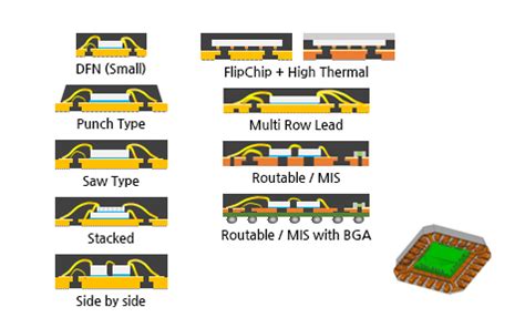
Types of QFN Packaging
QFN packages come in various types, each designed to cater to specific requirements and applications. Some of the most common types of QFN packaging include:
Standard QFN (SQFN)
The Standard QFN, also known as SQFN, is the most basic and widely used type of QFN packaging. It features a square or rectangular body with exposed pads on the bottom surface for thermal and electrical connection. The leads are located on the periphery of the package, providing a compact and low-profile solution.
Dual Row QFN (DRQFN)
Dual Row QFN packages feature two rows of leads on the package periphery, allowing for a higher pin count within the same package size as a Standard QFN. This type of QFN packaging is suitable for applications that require a higher level of integration and functionality.
Multi-Row QFN (MRQFN)
Multi-Row QFN packages take the concept of Dual Row QFN further by incorporating three or more rows of leads on the package periphery. This allows for an even higher pin count and greater flexibility in design, making it suitable for complex, high-performance applications.
Punch QFN (PQFN)
Punch QFN packages are manufactured using a punching process instead of the traditional sawing method. This results in a more robust and reliable package with better mechanical strength and improved moisture resistance. PQFN packages are commonly used in automotive and industrial applications that require high reliability.
Wettable Flank QFN (WFQFN)
Wettable Flank QFN packages feature a unique design that allows for improved solder joint inspection. The package leads have a wettable flank, which means that the solder can flow up the side of the lead, creating a visible solder joint. This enhances the reliability and quality control of the assembly process.

QFN Package Assembly Process
The assembly process for QFN packages involves several key steps to ensure reliable and efficient attachment to the PCB. The main stages of the QFN assembly process are:
- Solder Paste Application
- Package Placement
- Reflow Soldering
- Inspection and Testing
Solder Paste Application
The first step in the QFN assembly process is the application of solder paste to the PCB pads. This is typically done using a stencil printing method, where a metal stencil with apertures corresponding to the PCB pads is placed over the board. Solder paste is then applied onto the stencil and spread using a squeegee, depositing the paste onto the pads through the apertures.
Package Placement
Once the solder paste is applied, the QFN package is placed onto the PCB using a pick-and-place machine. The machine uses computer vision and precision mechanics to accurately position the package on the pads, ensuring proper alignment with the solder paste deposits.
Reflow Soldering
After package placement, the PCB undergoes a reflow soldering process. The board is heated in a reflow oven, following a specific temperature profile that allows the solder paste to melt, flow, and form a reliable connection between the package leads and the PCB pads. The reflow profile must be carefully controlled to ensure optimal solder joint formation and to prevent thermal damage to the components.
Inspection and Testing
Following the reflow soldering process, the assembLED PCB undergoes inspection and testing to verify the quality and reliability of the solder joints. This may include visual inspection, X-ray imaging, and electrical testing to ensure proper connectivity and performance.

Benefits of QFN Packaging
QFN packaging offers numerous benefits over traditional packaging methods, making it an attractive choice for a wide range of applications. Some of the key advantages of QFN packaging include:
Reduced Package Size
QFN packages have a smaller footprint compared to other surface-mount packages, such as QFP (Quad Flat Package) and BGA (Ball Grid Array). This allows for higher component density on the PCB, enabling the design of more compact and lightweight electronic devices.
Improved Thermal Performance
The exposed pad on the bottom of the QFN package provides an efficient thermal path for heat dissipation. This allows for better thermal management of the device, reducing the risk of overheating and improving overall system reliability.
Enhanced Electrical Performance
QFN packages offer improved electrical performance due to their shorter lead lengths and reduced parasitic inductance and capacitance. This results in faster signal propagation, lower signal distortion, and better high-frequency performance, making QFN packaging suitable for high-speed and RF applications.
Cost-Effectiveness
QFN packaging is a cost-effective solution compared to other packaging methods. The smaller package size reduces material costs, while the simplified assembly process and higher component density on the PCB contribute to lower manufacturing costs.
Reliability
QFN packages offer excellent reliability due to their robust construction and the use of advanced assembly techniques. The exposed pad provides a strong mechanical anchor to the PCB, reducing the risk of package delamination and improving solder joint reliability.

Frequently Asked Questions (FAQ)
1. What is the difference between QFN and QFP packaging?
QFN (Quad Flat No-lead) and QFP (Quad Flat Package) are both Surface-Mount Packaging technologies, but they differ in their design and lead configuration. QFN packages have a smaller footprint and no leads extending from the package body, while QFP packages have leads that extend from all four sides of the package. QFN packages offer better thermal and electrical performance, while QFP packages are suitable for applications that require higher pin counts and easier visual inspection of solder joints.
2. Can QFN packages be soldered using traditional through-hole techniques?
No, QFN packages are designed specifically for surface-mount assembly and cannot be soldered using through-hole techniques. The packages lack the long leads required for through-hole mounting and are intended to be soldered directly onto the surface of the PCB using reflow Soldering Methods.
3. How does the exposed pad in QFN packages improve thermal performance?
The exposed pad on the bottom of the QFN package acts as a thermal conductor, providing a direct path for heat to flow from the device to the PCB. This allows for more efficient heat dissipation compared to packages without an exposed pad, where the heat must be conducted through the package leads. By improving thermal performance, the exposed pad helps to reduce the risk of device overheating and enhances overall system reliability.
4. Are there any specific design considerations for PCBs using QFN packages?
Yes, when designing PCBs for QFN packages, there are several key considerations to ensure optimal performance and reliability:
- Proper pad sizing and spacing to accommodate the package dimensions and solder joint formation
- Appropriate solder mask design to prevent solder bridging between pads
- Thermal pad design to ensure efficient heat dissipation from the package to the PCB
- Correct solder paste stencil aperture design to deposit the right amount of solder paste for each pad
- Consideration of PCB material and layer stack-up to manage thermal and electrical performance
5. What are the challenges associated with inspecting QFN solder joints?
Inspecting solder joints in QFN packages can be challenging due to the lack of visible leads extending from the package body. Traditional visual inspection methods may not provide a clear view of the Solder Joint Quality. To overcome this challenge, several techniques can be employed:
- X-ray inspection: X-ray imaging allows for a non-destructive view of the solder joints beneath the package, enabling the detection of voids, bridging, or other defects.
- Wettable flank QFN (WFQFN): The wettable flank design allows solder to flow up the side of the package lead, creating a visible solder joint that can be inspected using standard visual methods.
- Boundary scan testing: Boundary scan techniques, such as JTAG, can be used to verify the electrical connectivity of the solder joints without relying on visual inspection.
By understanding these challenges and employing appropriate inspection techniques, manufacturers can ensure the quality and reliability of QFN solder joints.
Conclusion
QFN packaging has revolutionized the electronics industry, offering a compact, high-performance, and cost-effective solution for a wide range of applications. By understanding the various types of QFN packages, the assembly process, and the benefits they offer, designers and manufacturers can make informed decisions when selecting packaging technologies for their products.
As electronic devices continue to become smaller, faster, and more complex, QFN packaging will play an increasingly important role in enabling the development of advanced, reliable, and efficient systems. By staying up-to-date with the latest advancements in QFN technology and best practices for assembly and inspection, the electronics industry can continue to push the boundaries of innovation and deliver cutting-edge products to consumers worldwide.


Leave a Reply