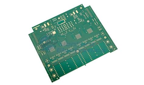
What are HDI PCBs?
High-Density Interconnect (HDI) PCBs are advanced printed circuit boards that feature higher wiring density per unit area compared to conventional PCBs. This is achieved through the use of smaller vias, finer traces, and capture pads, as well as by incorporating buried and blind vias. HDI PCBs enable the miniaturization of electronic devices while enhancing their functionality and performance.
Key features of HDI PCBs:
- Higher interconnect density
- Smaller vias and capture pads
- Finer trace widths and spacing
- Incorporation of buried and blind vias
- Reduced layer count and board thickness
Benefits of using HDI PCBs
HDI PCBs offer several advantages over traditional PCBs, making them an attractive choice for various applications:
-
Miniaturization: The higher wiring density allows for smaller form factors, enabling the design of compact electronic devices.
-
Improved signal integrity: Shorter signal paths and reduced layer count minimize signal distortion and crosstalk, resulting in better signal integrity.
-
Enhanced thermal management: The use of blind and buried vias improves Thermal dissipation, preventing hotspots and ensuring reliable operation.
-
Increased reliability: HDI PCBs exhibit better mechanical strength and reduced susceptibility to vibrations and shocks.
-
Cost-effectiveness: Although the initial fabrication costs may be higher, HDI PCBs often lead to overall cost savings by reducing the number of layers and the size of the final product.

HDI PCB Manufacturing Process
The manufacturing process of HDI PCBs involves several key steps:
-
Material selection: Choose high-quality substrate materials, such as FR-4, with suitable dielectric properties and thermal stability.
-
Patterning: Create the desired circuit pattern using photolithography or laser direct imaging (LDI) techniques.
-
Drilling: Drill through-holes, blind vias, and buried vias using mechanical or laser drilling methods.
-
Plating: Plate the drilled holes and vias with copper to establish electrical connections between layers.
-
Lamination: Laminate the individual layers together using heat and pressure to form a multi-layer PCB.
-
Surface finishing: Apply a surface finish, such as ENIG (Electroless Nickel Immersion Gold) or HASL (Hot Air Solder Leveling), to protect the exposed copper and improve solderability.
-
Electrical testing: Perform electrical tests to ensure the functionality and reliability of the manufactured HDI PCB.

HDI PCB Design Considerations
When designing HDI PCBs, several factors should be taken into account to ensure optimal performance and manufacturability:
-
Via types and sizes: Choose the appropriate via types (through-hole, blind, or buried) and sizes based on the design requirements and manufacturing capabilities.
-
Trace width and spacing: Adhere to the minimum trace width and spacing guidelines to maintain signal integrity and prevent short circuits.
-
Layer stackup: Design an optimal layer stackup that minimizes the number of layers while ensuring proper signal routing and power distribution.
-
Impedance control: Implement controlled impedance techniques to maintain consistent impedance along the signal paths, minimizing reflections and signal distortion.
-
Thermal management: Incorporate adequate thermal management strategies, such as the use of thermal vias and proper copper balancing, to dissipate heat effectively.
-
DFM guidelines: Follow Design for Manufacturability (DFM) guidelines to ensure the HDI PCB design is compatible with the chosen manufacturing process and tolerances.

Applications of HDI PCBs
HDI PCBs find applications in a wide range of industries and products, including:
-
Consumer electronics: Smartphones, tablets, smartwatches, and other portable devices.
-
Automotive: Advanced driver assistance systems (ADAS), infotainment systems, and vehicle control units.
-
Medical devices: Implantable devices, diagnostic equipment, and wearable health monitors.
-
Aerospace and defense: Avionics systems, radar modules, and satellite communication devices.
-
Industrial automation: Robotics, process control systems, and IoT devices.
HDI PCB Industry Trends and Future Outlook
The HDI PCB market is expected to grow significantly in the coming years, driven by the increasing demand for miniaturized and high-performance electronic devices. Some key trends shaping the industry include:
-
Advanced materials: The development of new substrate materials with improved thermal, mechanical, and electrical properties will enable the fabrication of more complex and reliable HDI PCBs.
-
5G and IoT: The proliferation of 5G networks and the Internet of Things (IoT) will drive the demand for HDI PCBs in various applications, such as smart homes, connected vehicles, and industrial IoT.
-
Embedded components: The integration of passive and active components within the PCB substrate will further enhance the miniaturization and functionality of HDI PCBs.
-
Advanced manufacturing techniques: The adoption of advanced manufacturing technologies, such as 3D printing and laser-based processes, will enable the production of more intricate and high-precision HDI PCBs.
As the electronics industry continues to evolve, HDI PCBs will play a crucial role in enabling the development of cutting-edge technologies and shaping the future of electronic devices.
HDI PCB Manufacturing Capabilities
The manufacturing capabilities of HDI PCBs have significantly advanced in recent years, allowing for the production of more complex and high-density designs. The following table summarizes some of the key manufacturing capabilities:
| Parameter | Typical Value |
|---|---|
| Minimum via diameter | 50-100 µm |
| Minimum via pad diameter | 100-150 µm |
| Minimum trace width | 50-75 µm |
| Minimum trace spacing | 50-75 µm |
| Maximum aspect ratio | 1:1 to 1:1.5 |
| Minimum Annular Ring | 25-50 µm |
| Maximum layer count | 12-16 layers |
Note: These values are approximate and may vary depending on the specific manufacturing process and fabrication facility.
As HDI PCB technology continues to advance, these manufacturing capabilities are expected to improve further, enabling the production of even more complex and high-density designs.
Frequently Asked Questions (FAQ)
-
What is the difference between HDI PCBs and conventional PCBs?
HDI PCBs feature higher wiring density per unit area compared to conventional PCBs. They incorporate smaller vias, finer traces, and capture pads, as well as buried and blind vias, enabling miniaturization and improved performance. -
What are the benefits of using HDI PCBs in electronic devices?
The benefits of using HDI PCBs include miniaturization, improved signal integrity, enhanced thermal management, increased reliability, and cost-effectiveness. -
What are the key design considerations for HDI PCBs?
When designing HDI PCBs, important factors to consider include via types and sizes, trace width and spacing, layer stackup, impedance control, thermal management, and adherence to DFM guidelines. -
In which industries are HDI PCBs commonly used?
HDI PCBs find applications in various industries, such as consumer electronics, automotive, medical devices, aerospace and defense, and industrial automation. -
What are the future trends in the HDI PCB industry?
The future of the HDI PCB industry is shaped by trends such as the development of advanced materials, the proliferation of 5G and IoT, the integration of embedded components, and the adoption of advanced manufacturing techniques like 3D printing and laser-based processes.
In conclusion, High-Density Interconnect (HDI) PCBs represent a significant advancement in printed circuit board technology, offering numerous benefits and enabling the development of cutting-edge electronic devices across various industries. As the demand for miniaturization and high-performance electronics continues to grow, HDI PCBs will play an increasingly crucial role in shaping the future of the electronics industry.


Leave a Reply