Introduction to PCB soldering
Soldering is an essential skill for anyone working with electronic circuits and printed circuit boards (PCBs). PCB soldering involves joining electronic components to the copper pads on a PCB using a molten metal alloy called solder. Proper soldering technique ensures a strong electrical and mechanical connection between the components and the board, which is crucial for the proper functioning and reliability of the electronic device.
In this comprehensive guide, we will cover everything you need to know about PCB soldering, including the tools and materials required, safety precautions, and step-by-step instructions for various soldering techniques.
Tools and Materials Required for PCB Soldering
Before you start soldering, it is important to gather all the necessary tools and materials. Here is a list of the essential items you will need:
- Soldering iron
- Soldering iron stand
- Solder wire (lead-based or lead-free)
- Flux (optional)
- Solder wick or desoldering pump
- Tweezers
- Wire cutters
- Multimeter
- Isopropyl alcohol and cleaning cloth
- Safety glasses
- Ventilated workspace
Choosing the Right Soldering Iron
A soldering iron is the most important tool for PCB soldering. When selecting a soldering iron, consider the following factors:
- Wattage: A soldering iron with a wattage between 20W and 60W is suitable for most PCB soldering tasks.
- Temperature control: Look for a soldering iron with adjustable temperature control to accommodate different types of solder and components.
- Tip size and shape: Choose a soldering iron tip that matches the size of the components and pads on your PCB. Common tip shapes include conical, chisel, and fine point.
Solder Wire Types
Solder wire comes in two main types: lead-based and lead-free. Lead-based solder is easier to work with but is being phased out due to environmental and health concerns. Lead-free solder has a higher melting point and requires more skill to use effectively.
When choosing solder wire, also consider the diameter. A diameter between 0.5mm and 1.0mm is suitable for most PCB soldering applications.

Safety Precautions for PCB Soldering
Soldering involves high temperatures and potentially harmful fumes, so it is essential to take proper safety precautions:
- Always wear safety glasses to protect your eyes from solder splashes and fumes.
- Work in a well-ventilated area or use a fume extractor to minimize exposure to solder fumes.
- Keep the soldering iron in its stand when not in use to avoid accidental burns.
- Never touch the tip of the soldering iron or the molten solder.
- Wash your hands thoroughly after soldering, especially before eating or drinking.

Step-by-Step Guide to PCB Soldering
Step 1: Preparing the Soldering Iron
- Plug in the soldering iron and set the temperature according to the type of solder you are using (lead-based or lead-free).
- Wait for the soldering iron to reach the desired temperature. This usually takes a few minutes.
- Clean the tip of the soldering iron with a damp sponge or brass wool to remove any oxidation or residue.
- Tin the tip of the soldering iron by applying a small amount of solder to it. This helps improve heat transfer and prevents oxidation.
Step 2: Preparing the PCB and Components
- Place the PCB in a PCB holder or on a non-conductive surface.
- Identify the location of each component based on the PCB layout diagram.
- Bend the leads of the through-hole components to fit the hole spacing on the PCB.
- Insert the components into their respective holes, ensuring they are fully seated against the PCB.
Step 3: Soldering Through-Hole Components
- Place the tip of the soldering iron against the component lead and the PCB pad simultaneously.
- Apply a small amount of solder to the joint, allowing it to melt and flow around the lead and pad.
- Remove the solder wire and then the soldering iron, keeping the joint still until the solder solidifies.
- Trim the excess component leads with wire cutters, leaving about 1-2mm of lead above the solder joint.
Step 4: Soldering Surface Mount Components
- Apply a small amount of solder paste or flux to the PCB pads where the surface mount component will be placed.
- Position the component on the pads using tweezers, ensuring proper alignment.
- Place the tip of the soldering iron against the component lead and the PCB pad simultaneously.
- Apply a small amount of solder to the joint, allowing it to melt and flow around the lead and pad.
- Remove the soldering iron and let the solder joint cool and solidify.
Step 5: Inspecting and Cleaning the Solder Joints
- Visually inspect each solder joint for proper wetting, shape, and size. A good solder joint should be shiny, smooth, and concave.
- Use a multimeter to test for continuity and shorts between adjacent pins or pads.
- Clean any flux residue from the PCB using isopropyl alcohol and a clean cloth.
 ILPIAUuKBRQAUUUtACUuKWigAooopDCiiigAooooAKKKKACiiigAooooAKKKKACiiigAooooAKKKKACiiigAooooAKKKKACiiigAooooATFOpKWgDzYj5j26VMG4/nTSOeRR0+leLY9clGKcSAOKYOlIXGKaEyQNgdeaglm28Dlj29KimuPLG0cuew7fWmwoXOW5J710U6fU551OiJ4Yi5BPJrXtrcYBNQWsPK/hWzDGAK7UjkbHxRhR+FTgUKMU6qEAFOA6UAU4CmIKdtpQBS0CCilxRQAnWnAYFAWnUwEoopaYBRilooEFFFLQAUtFFIYUUUUAFFFFABRRRQAUUUUAFFFFABRRRQAUUUUAFFFFABRRRQAUUUUAFFFFABRRRQAUUUUAFFFFABRRRQAlLRRQAUtJS0AeeN1NMqMucmq1zeQ2qGSVwOuFz8zewFeQl2PVuXC4UEsQABk56Vny6irMUt/mIyC/YduKx5L+6vWxykWeEB5P8AvGrtrDwOK2hBdTGci3CjM2WJJPU+prXtos44qrbxdOK27ODpXXFHLJlu2iwF4rQRcVHFGABU4GKtIgWlFAFOAqhC04CkAp1AhaWkpaAFpQKAKdTEJRS0UwEpaKKACloxS0AJiloopDCiiigAooooAKKKKACiiigAooooAKKKKACiiigAooooAKKKKACiiigAooooAKKKKACiiigAooooAKKKKACiiigAoopDQAU6m06gDxO815MFLUEsR99uAPoKxy89y+6V2Zj13f0qFELGtW1tSe36VwqKWx6DdiWzgPFb1tD93iorW2xt47Vt2tsTjitYxMJSJrW3zjitmCHYBUdvBtUcVeVQMVsY3FUYFPApAKcBTJFApwFIBTwKYgFLRS4oASnAUlPpgKKKKKYgooooAKXFFLSGFFFFABRRRQAUUUUAFFFFABRRRQAUUUUAFFFFABRRRQAUUUUAFFFFABRRRQAUUUUAFFFFABRRRQAUUUUAFFFFABRRRQAUUUUAFIaKSgBadTKfTEeF21pyMg9a3bW1AxxT7e0wenf0ratbTOOK5YxOqUhtraZxxW1b26qBxToLcJg1bAxWyVjFtigDpTwKaAeKkApkiinCkApwFMBwpaKKBAKWinAUAAp2aSlqhBRRRQAUtFLQAUUUUhhRRRQAUUUUAFFFFABRRRQAUUUUAFFFFABRRRQAUUUUAFFFFABRRRQAUUUUAFFFFABRRRQAUUUUAFFFFABRRRQAlLRRQAUUnNFABmkoopiCn0yn0AcHbKuRwO3atu2Vf7o/IUUVjE0kXgBxwKeAPQUUVQug8AegpygegoopoQ8Aegp4A9B+VFFMQYHoKXA9BRRQAuB6D8qcAMdBRRTAXA9BRgegoooAMD0FGB6UUUAGB6UUUUAFFFFABRRRQAUUUUAFHFFFABxRRRQAUUUUAFFFFABRRRQAUUUUAFFFFABRRRQAUUUUAFFFFABRRRQAUcUUUAHFHFFFABxRxRRQAUUUUAGB6UYHoKKKADA9BRgegoooAMD0FNJOTRRQI//Z” alt=”” class=”wp-image-136″ >
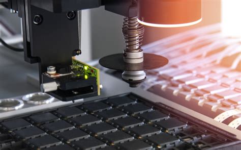
Common PCB Soldering Techniques
Drag Soldering
Drag soldering is a technique used for soldering multiple pins or leads in a row, such as those found on Integrated Circuits (ICs) or connectors.
- Apply a small amount of solder to the tip of the soldering iron.
- Drag the soldering iron tip across the pins and pads, maintaining contact with both surfaces.
- The solder should flow evenly across all the pins and pads, creating a continuous joint.
Reflow Soldering
Reflow soldering is a technique used for soldering surface mount components using solder paste and a heat source, such as a hot air gun or reflow oven.
- Apply solder paste to the PCB pads using a stencil or syringe.
- Place the surface mount components on the pads, ensuring proper alignment.
- Heat the PCB and components using a hot air gun or reflow oven, following the recommended temperature profile for the solder paste.
- The solder paste will melt and flow around the component leads and pads, creating a strong solder joint.
Troubleshooting Common PCB Soldering Issues
Cold Solder Joints
A cold solder joint occurs when the solder does not melt completely, resulting in a weak and unreliable connection. Symptoms of a cold solder joint include:
- Dull, grainy, or pitted appearance
- Poor wetting of the component lead or PCB pad
- High electrical resistance
To fix a cold solder joint, reheat the joint with the soldering iron and apply additional solder if necessary.
Solder Bridges
A solder bridge is an unintended connection between two or more solder joints, often caused by using too much solder or improper soldering technique. To remove a solder bridge:
- Apply flux to the affected area.
- Use a solder wick or desoldering pump to remove the excess solder.
- Resolder the joints if necessary, using the correct amount of solder.
Overheated Components
Overheating components during soldering can cause damage, such as lifted pads, burnt markings, or reduced performance. To prevent overheating:
- Use the lowest suitable temperature for your soldering iron.
- Minimize the time the soldering iron is in contact with the component and PCB.
- Use heat sinks or thermal shunts to protect sensitive components.
FAQ
1. What is the difference between lead-based and lead-free solder?
Lead-based solder contains a mixture of tin and lead, typically in a ratio of 60/40 or 63/37. It has a lower melting point and is easier to work with compared to lead-free solder. However, due to environmental and health concerns, lead-based solder is being phased out in favor of lead-free alternatives.
Lead-free solder is typically made from a mixture of tin, silver, and copper (SAC alloys). It has a higher melting point and requires more precise temperature control during soldering. While lead-free solder is more environmentally friendly, it can be more challenging to work with and may require additional training and practice.
2. How do I choose the right soldering iron tip for my PCB?
When choosing a soldering iron tip for your PCB, consider the following factors:
- Size: The tip should be appropriate for the size of the components and pads on your PCB. A larger tip may be suitable for bigger components or ground planes, while a smaller tip is better for fine-pitch components and tight spaces.
- Shape: Common tip shapes include conical, chisel, and fine point. Chisel tips are versatile and suitable for most soldering tasks, while fine point tips are ideal for precision work.
- Material: Soldering iron tips are typically made from copper or a copper alloy, which provides good heat conductivity. Some tips may have an iron or nickel plating to improve durability and reduce oxidation.
It’s a good idea to have a variety of tip sizes and shapes available to accommodate different soldering tasks and PCB layouts.
3. What is the purpose of using flux in PCB soldering?
Flux is a chemical compound that helps improve the soldering process by:
- Removing oxidation and contamination from the surfaces to be soldered, promoting better wetting and adhesion of the solder.
- Preventing further oxidation during the soldering process.
- Improving the flow and spread of the molten solder, resulting in a stronger and more reliable solder joint.
Flux can be applied directly to the PCB and components or may be included in the core of the solder wire (rosin-core solder). After soldering, any remaining flux residue should be cleaned from the PCB using isopropyl alcohol to prevent corrosion or other issues.
4. How can I tell if a solder joint is good or bad?
A good solder joint should have the following characteristics:
- Shiny and smooth surface
- Concave shape that resembles a volcano or fillet
- Good wetting and adhesion to the component lead and PCB pad
- No visible cracks, pits, or voids
A bad solder joint may exhibit:
- Dull, grainy, or pitted appearance (cold joint)
- Bulbous or convex shape (too much solder)
- Poor wetting or adhesion to the surfaces (insufficient heat or contamination)
- Cracks, gaps, or voids (mechanical stress or overheating)
If you suspect a solder joint is bad, you can use a multimeter to test for continuity and resistance. If necessary, reheat the joint with the soldering iron and apply additional solder or remove excess solder using a solder wick or desoldering pump.
5. What safety precautions should I take when soldering PCBs?
When soldering PCBs, it’s essential to take the following safety precautions:
- Wear safety glasses to protect your eyes from solder splashes and fumes.
- Work in a well-ventilated area or use a fume extractor to minimize exposure to solder fumes, which can contain harmful chemicals.
- Use a soldering iron stand to hold the hot iron when not in use, preventing accidental burns or fires.
- Never touch the tip of the soldering iron or the molten solder, as they can cause severe burns.
- Wash your hands thoroughly after soldering, especially before eating or drinking, to avoid ingesting any harmful residues.
- Keep your workspace clean and organized to prevent accidents and contamination of the PCB or components.
- Properly dispose of any solder waste, such as used solder wicks or clipped component leads, in accordance with local regulations.
By following these safety guidelines, you can protect yourself and others from potential hazards associated with PCB soldering.
Conclusion
PCB soldering is a crucial skill for anyone working with electronic circuits and devices. By understanding the tools, materials, and techniques involved in soldering, you can create strong and reliable connections between components and the PCB. Remember to prioritize safety, practice proper soldering techniques, and take the time to inspect and clean your solder joints for the best results.
With patience and practice, you’ll soon be able to confidently tackle any PCB soldering project, from simple repairs to complex prototypes. Happy soldering!


Leave a Reply