What is Altium Designer?
Altium Designer is a powerful, integrated PCB design environment that combines schematic capture, PCB layout, and manufacturing output generation into a single, user-friendly package. It is widely used by professional engineers, hobbyists, and students alike for designing printed circuit boards across various industries, including consumer electronics, aerospace, and telecommunications.
Key Features of Altium Designer
| Feature | Description |
|---|---|
| Schematic Capture | Create, edit, and manage schematic diagrams with a comprehensive library of components and symbols. |
| PCB Layout | Design PCB layouts with advanced routing tools, 3D visualization, and real-time design rule checking. |
| Library Management | Organize and manage component libraries, footprints, and design templates. |
| Manufacturing Output Generation | Generate manufacturing files, such as Gerber, NC drill, and pick-and-place files, for seamless communication with PCB Fabrication and assembly providers. |
Getting Started with Altium Designer
System Requirements
Before installing Altium Designer, ensure that your computer meets the following minimum system requirements:
| Component | Minimum Requirement |
|---|---|
| Operating System | Windows 10 (64-bit) |
| Processor | Intel Core i5 or equivalent |
| RAM | 8 GB |
| Storage | 10 GB of free disk space |
| Graphics | DirectX 11 compatible graphics card with at least 1 GB of dedicated memory |
Installing Altium Designer
To install Altium Designer, follow these steps:
- Download the Altium Designer installer from the official Altium website (https://www.altium.com/products/downloads).
- Run the installer and follow the on-screen instructions.
- Activate your Altium Designer license by entering your license key or signing in with your Altium account.

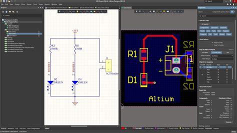
Navigating the Altium Designer Interface
Main Window
Upon launching Altium Designer, you’ll be greeted with the main window, which consists of several key areas:
- Menus and Toolbars
- Panels
- Design Workspace
- Status Bar
Menus and Toolbars
The menus and toolbars provide access to various commands and tools for creating and editing your designs. The most commonly used menus include:
- File: Create, open, save, and close projects and documents.
- Edit: Perform basic editing tasks, such as cut, copy, paste, and undo/redo.
- View: Customize the appearance of the Altium Designer interface and toggle the visibility of panels and toolbars.
- Design: Access tools for creating and editing schematics, PCBs, and libraries.
- Tools: Configure Altium Designer settings and access additional tools, such as the Component Wizard and the Manufacturer Part Search.
Panels
Panels are dockable windows that provide access to various tools, libraries, and design information. Some of the most important panels include:
- Projects: Manage project files, design documents, and libraries.
- Properties: View and edit properties of selected objects in the design workspace.
- SCH Library: Access schematic symbol libraries.
- PCB Library: Access PCB footprint libraries.
- Messages: View design rule check (DRC) warnings, errors, and other notifications.
Design Workspace
The design workspace is the central area where you create and edit your schematic diagrams and PCB layouts. You can switch between the schematic and PCB editors using the tabs at the bottom of the workspace.
Customizing the Interface
Altium Designer allows you to customize the interface to suit your preferences and workflow. To customize the interface:
- Go to “View” > “Workspace Panels” to toggle the visibility of individual panels.
- Right-click on the menu or toolbar area and select “Customize” to add, remove, or rearrange buttons and commands.
- Go to “Tools” > “Preferences” to configure various settings, such as color schemes, hotkeys, and design rule defaults.

Creating a New Project
To create a new project in Altium Designer:
- Go to “File” > “New” > “Project” or press “Ctrl+N”.
- In the “New Project” dialog box, select “PCB Project” and click “OK”.
- Choose a location to save your project and give it a name.
- Click “Save” to create the new project.
Your new project will appear in the Projects panel, ready for you to start adding design documents.

Creating a Schematic
To create a new schematic in your project:
- Right-click on your project in the Projects panel and select “Add New to Project” > “Schematic”.
- In the “New Schematic” dialog box, give your schematic a name and click “OK”.
The schematic editor will open, allowing you to start designing your circuit.
Adding Components
To add components to your schematic:
- Press “P” to open the “Libraries” panel.
- Browse or search for the desired component in the available libraries.
- Drag and drop the component from the library onto your schematic.
- Repeat for all necessary components.
Wiring Components
To wire components together:
- Select the “Wire” tool from the toolbar or press “W”.
- Click on the first pin you want to connect.
- Move the cursor to the second pin and click to complete the connection.
- Repeat for all necessary connections.
Annotating Components
To annotate components with unique designators:
- Go to “Tools” > “Annotation”.
- In the “Annotate” dialog box, select the desired annotation options and click “OK”.
Design Rule Checking
To check your schematic for errors:
- Go to “Tools” > “Design Rule Check”.
- In the “Design Rule Check” dialog box, select the desired rules and click “Run DRC”.
- Review any warnings or errors in the Messages panel and make necessary corrections.
Creating a PCB Layout
To create a PCB layout from your schematic:
- Go to “Design” > “Update PCB Document” > “Create PCB from Schematic”.
- In the “Engineering Change Order” dialog box, review the changes and click “Execute Changes”.
The PCB editor will open with your components placed on the board.
Placing Components
To place components on your PCB:
- Select a component in the PCB editor.
- Use the “Move” tool or press “M” to position the component on the board.
- Repeat for all components.
Routing Traces
To route traces between components:
- Select the “Interactive Routing” tool from the toolbar or press “Shift+R”.
- Click on a pad to start the trace.
- Move the cursor to guide the trace, clicking to add vertices as needed.
- Double-click or press “Enter” to complete the trace.
- Repeat for all necessary connections.
Applying Design Rules
To apply design rules to your PCB layout:
- Go to “Design” > “Rules”.
- In the “PCB Rules and Constraints Editor” dialog box, create or modify rules for track width, clearance, via size, and other parameters.
- Click “Apply” and “OK” to enforce the rules on your PCB layout.
Design Rule Checking
To check your PCB layout for errors:
- Go to “Tools” > “Design Rule Check”.
- In the “Design Rule Check” dialog box, select the desired rules and click “Run DRC”.
- Review any warnings or errors in the Messages panel and make necessary corrections.
Generating Manufacturing Outputs
To generate manufacturing files for your PCB:
- Go to “File” > “Fabrication Outputs” > “Gerber Files”.
- In the “Gerber Setup” dialog box, select the desired layers and settings, then click “OK”.
- Choose a location to save the Gerber files and click “OK”.
Repeat the process for other necessary manufacturing files, such as NC drill and pick-and-place files.
Frequently Asked Questions (FAQ)
-
Can I use Altium Designer for free?
Altium Designer offers a free trial version that allows you to explore the software’s features for a limited time. However, for long-term use, you will need to purchase a license. -
Is Altium Designer compatible with other PCB design software?
Altium Designer can import and export various file formats, such as Gerber, ODB++, and IPC-2581, which enables compatibility with other PCB design software and manufacturing processes. -
What resources are available for learning Altium Designer?
Altium provides extensive documentation, tutorials, and video courses through its online learning platform, Altium Academy. Additionally, there are numerous third-party resources, such as books, online forums, and YouTube tutorials, that can help you learn Altium Designer. -
Can I create custom component libraries in Altium Designer?
Yes, Altium Designer allows you to create and manage custom component libraries. You can create schematic symbols, PCB footprints, and 3D models for your components and organize them in libraries for easy access and reuse across projects. -
How can I collaborate with others on Altium Designer projects?
Altium Designer offers a collaboration platform called Altium 365, which enables real-time collaboration, version control, and secure sharing of design data. With Altium 365, team members can work together on projects, regardless of their location, and maintain a single source of truth for their design files.
By following this tutorial and exploring the various features and resources available, you’ll be well on your way to mastering Altium Designer and creating professional-quality PCB designs. Remember to practice regularly, consult the documentation when needed, and engage with the Altium Designer community to continue learning and improving your skills.


Leave a Reply