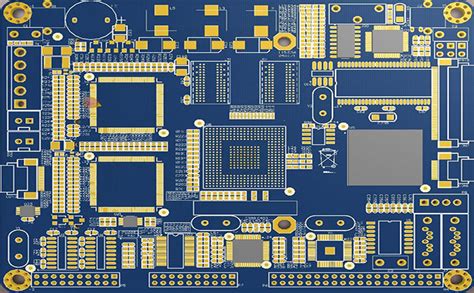
What is HDI PCB?
HDI (High Density Interconnect) PCB is a printed circuit board that features a higher wiring density per unit area than conventional PCBs. This is achieved through the use of smaller vias, finer traces, and capture pads, as well as by incorporating multiple layers of circuitry within the board. HDI PCBs enable the miniaturization of electronic devices while maintaining or enhancing their functionality and performance.
Key Features of HDI PCBs
- Microvias: HDI PCBs utilize microvias, which are small holes drilled through one or more layers of the PCB, typically with a diameter less than 150 microns.
- Fine pitch traces: The width and spacing of traces on HDI PCBs are significantly reduced compared to traditional PCBs, allowing for higher routing density.
- Blind and buried vias: HDI PCBs often incorporate blind vias (connecting an outer layer to an inner layer) and buried vias (connecting inner layers) to maximize space utilization.
- Sequential Lamination: The fabrication process for HDI PCBs involves sequential lamination of multiple layers, enabling the creation of complex, high-density designs.
Benefits of HDI PCBs
Space Saving and Miniaturization
One of the primary advantages of HDI PCBs is their ability to accommodate a high number of components and interconnects within a limited space. By utilizing smaller vias, finer traces, and multiple layers, HDI PCBs enable the miniaturization of electronic devices without compromising functionality or performance. This is particularly important in applications such as smartphones, wearables, and IoT devices, where compact size is a critical factor.
Improved Signal Integrity
HDI PCBs offer improved signal integrity compared to traditional PCBs due to several factors:
- Shorter signal paths: The compact layout of HDI PCBs results in shorter signal paths, reducing the risk of signal degradation and interference.
- Controlled impedance: HDI PCBs allow for better control over impedance, ensuring consistent signal quality and minimizing reflections and crosstalk.
- Reduced electromagnetic interference (EMI): The close proximity of components and the use of shielding techniques in HDI PCBs help to minimize EMI, enhancing overall signal integrity.
Enhanced Thermal Management
HDI PCBs provide better thermal management than traditional PCBs due to the following reasons:
- Increased copper coverage: HDI PCBs typically have a higher percentage of copper coverage, which helps to dissipate heat more effectively.
- Thermal vias: The use of thermal vias in HDI PCBs allows for efficient heat transfer from components to the board’s outer layers, where it can be dissipated through cooling solutions.
- Reduced thermal resistance: The compact layout and shorter signal paths in HDI PCBs result in lower thermal resistance, enabling better heat dissipation and preventing hotspots.
Cost Reduction in the Long Run
Although the initial design and fabrication costs for HDI PCBs may be higher than traditional PCBs, they offer cost savings in the long run:
- Fewer layers required: HDI PCBs can achieve the same functionality as traditional PCBs with fewer layers, reducing material costs.
- Smaller form factor: The miniaturization enabled by HDI PCBs leads to smaller overall device sizes, reducing packaging and shipping costs.
- Improved reliability: The enhanced signal integrity and thermal management of HDI PCBs contribute to improved reliability, reducing the risk of failures and associated repair or replacement costs.

HDI PCB Design Considerations
Layer Stack-up Planning
Proper layer stack-up planning is crucial for achieving a successful HDI PCB design. Consider the following factors:
- Number of layers: Determine the optimal number of layers based on the complexity of the design and the required functionality.
- Material selection: Choose appropriate materials for the dielectric layers and copper foils, considering factors such as dielectric constant, loss tangent, and thermal properties.
- Symmetry: Ensure that the layer stack-up is symmetrical to minimize warpage and stress during fabrication and assembly.
Via Types and Placement
HDI PCBs utilize various types of vias, each with specific design considerations:
- Microvias: Determine the appropriate microvia size and placement based on the design requirements and the capabilities of the fabrication process.
- Blind and buried vias: Strategically place blind and buried vias to maximize space utilization and minimize signal path lengths.
- Via-in-pad: Consider using via-in-pad technology to further increase component density and improve signal integrity.
Trace Width and Spacing
When designing HDI PCBs, it is essential to consider the following aspects related to trace width and spacing:
- Impedance control: Calculate the appropriate trace width and spacing to achieve the desired impedance for critical signals.
- Current carrying capacity: Ensure that the trace width is sufficient to handle the required current without excessive heating or voltage drop.
- Manufacturing constraints: Verify that the chosen trace width and spacing are compatible with the fabrication process and the manufacturer’s capabilities.
Component Placement and Routing
Optimize component placement and routing in HDI PCBs to achieve the best performance and manufacturability:
- Placement strategy: Group components based on their functional relationships and minimize the distance between interconnected components to reduce signal path lengths.
- Routing techniques: Employ routing techniques such as diagonal routing, meandering, and phase tuning to optimize signal integrity and minimize crosstalk.
- Design rule checks (DRC): Perform thorough DRCs to ensure that the design complies with the manufacturer’s guidelines and industry standards.

HDI PCB Fabrication Process
Sequential Lamination
HDI PCBs are fabricated using a sequential lamination process, which involves the following steps:
- Core layer fabrication: The core layers of the PCB are fabricated using standard PCB manufacturing techniques.
- Microvia drilling: Microvias are drilled through the core layers using laser or mechanical drilling methods.
- Plating and filling: The microvias are plated with copper and filled with a conductive material to create interconnects between layers.
- Additional layer lamination: Additional layers are laminated onto the core layers, and the process is repeated until the desired number of layers is achieved.
Laser Drilling
Laser drilling is a critical process in HDI PCB fabrication, enabling the creation of microvias with high precision and reliability:
- Laser types: UV and CO2 lasers are commonly used for drilling microvias, each with specific advantages and limitations.
- Process optimization: Laser drilling parameters, such as pulse duration, energy, and repetition rate, must be optimized to achieve the desired via size and quality.
- Cleaning and desmear: After laser drilling, the microvias undergo cleaning and desmear processes to remove debris and prepare the surfaces for plating.
Plasma Etching
Plasma etching is an essential process in HDI PCB fabrication, used for various purposes:
- Desmear: Plasma etching is used to remove the resin smear from the walls of microvias, ensuring proper electrical connection during plating.
- Surface preparation: Plasma etching can be used to prepare the surface of the PCB for better adhesion of subsequent layers or coatings.
- Trace formation: Plasma etching can be employed to create fine-pitch traces on the outer layers of the HDI PCB.

HDI PCB Testing and Inspection
Electrical Testing
Electrical testing is crucial to ensure the functionality and reliability of HDI PCBs:
- Continuity testing: Verify that all the intended connections are present and that there are no unintended short circuits.
- Insulation resistance testing: Measure the resistance between isolated conductors to ensure adequate insulation.
- High-potential (HiPot) testing: Apply a high voltage between conductors to detect any potential insulation breakdowns or leakage currents.
Optical Inspection
Optical inspection methods are used to visually examine HDI PCBs for defects and anomalies:
- Automated optical inspection (AOI): Use computer vision systems to quickly scan the PCB surface for defects such as missing components, solder bridges, or trace anomalies.
- Manual visual inspection: Employ trained operators to visually inspect the PCB under magnification, looking for defects that may have been missed by AOI.
- Microscopic inspection: Use high-magnification microscopes to examine critical areas of the PCB, such as microvias and fine-pitch traces, for any irregularities or defects.
X-ray Inspection
X-ray inspection is a non-destructive testing method that allows for the examination of internal features of HDI PCBs:
- Microvia inspection: Use X-ray imaging to verify the integrity of microvias, checking for proper plating, filling, and the absence of voids or cracks.
- BGA and CSP inspection: Employ X-ray inspection to examine the solder joints of ball grid array (BGA) and chip-scale package (CSP) components, ensuring proper alignment and connection.
- Automated X-ray inspection (AXI): Utilize computer-controlled X-ray systems to automatically scan and analyze the internal structure of HDI PCBs, identifying potential defects or anomalies.
Frequently Asked Questions (FAQ)
-
Q: What is the main difference between HDI PCBs and traditional PCBs?
A: The main difference between HDI PCBs and traditional PCBs lies in the higher wiring density per unit area achieved through the use of smaller vias, finer traces, and capture pads, as well as the incorporation of multiple layers of circuitry within the board. This enables HDI PCBs to accommodate more components and interconnects in a smaller space compared to traditional PCBs. -
Q: What are the typical applications of HDI PCBs?
A: HDI PCBs are commonly used in applications that require high functionality and performance in a compact form factor, such as smartphones, wearable devices, IoT devices, medical devices, aerospace and defense systems, and high-speed communication equipment. -
Q: What are the challenges associated with HDI PCB design and fabrication?
A: Some of the challenges associated with HDI PCB design and fabrication include the need for precise control over impedance, the complexity of the layer stack-up, the requirement for specialized equipment and processes (such as laser drilling and plasma etching), and the higher initial costs compared to traditional PCBs. -
Q: How do HDI PCBs improve signal integrity compared to traditional PCBs?
A: HDI PCBs improve signal integrity through shorter signal paths, better control over impedance, and reduced electromagnetic interference (EMI). The compact layout of HDI PCBs minimizes signal path lengths, reducing the risk of signal degradation and interference. Additionally, the close proximity of components and the use of shielding techniques help to minimize EMI, further enhancing signal integrity. -
Q: What are the key considerations when selecting a manufacturer for HDI PCBs?
A: When selecting a manufacturer for HDI PCBs, key considerations include the manufacturer’s experience and expertise in HDI PCB fabrication, their capability to handle the required design complexity and tolerances, their quality control processes and certifications, and their ability to provide reliable customer support and communication throughout the project.
| Parameter | HDI PCBs | Traditional PCBs |
|---|---|---|
| Via Size | < 150 μm | > 150 μm |
| Trace Width/Spacing | < 100 μm | > 100 μm |
| Layer Count | Higher | Lower |
| Component Density | Higher | Lower |
| Signal Integrity | Better | Good |
| Thermal Management | Better | Good |
| Initial Cost | Higher | Lower |
| Long-term Cost | Lower | Higher |
In conclusion, HDI PCBs offer numerous advantages over traditional PCBs, including higher component density, improved signal integrity, better thermal management, and long-term cost savings. However, achieving a perfect HDI PCB requires careful consideration of design factors, such as layer stack-up planning, via types and placement, trace width and spacing, and component placement and routing. Additionally, the fabrication process involves specialized techniques, such as sequential lamination, laser drilling, and plasma etching, which must be optimized to ensure the highest quality and reliability. Thorough testing and inspection, including electrical testing, optical inspection, and X-ray inspection, are essential to verify the functionality and integrity of the final product. By understanding these key aspects and partnering with an experienced and reliable HDI PCB manufacturer, designers and engineers can unlock the full potential of HDI technology and create innovative, high-performance electronic devices.


Leave a Reply