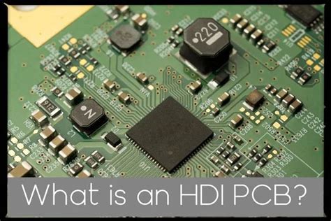
What is HDI PCB?
HDI PCB, or High Density Interconnect Printed Circuit Board, is a type of PCB that features a higher wiring density per unit area than conventional PCBs. This is achieved through the use of smaller vias, finer trace widths and spaces, and more precise layer-to-layer registration. HDI PCBs allow for the miniaturization of electronic devices while maintaining or even improving their functionality and performance.
Key Features of HDI PCBs
- Smaller vias (microvias) with diameters less than 150 µm
- Finer trace widths and spaces, typically less than 100 µm
- Higher layer counts (8 or more)
- Thin dielectric materials for reduced overall thickness
- Buried and blind vias for increased interconnect density
- Sequential Lamination process for fabrication
Advantages of HDI PCBs
HDI PCBs offer several advantages over traditional PCBs:
-
Miniaturization: The higher wiring density allows for smaller form factors, enabling the design of more compact electronic devices.
-
Improved Signal Integrity: Shorter signal paths and reduced layer-to-layer transitions lead to improved signal integrity and reduced noise and crosstalk.
-
Increased Functionality: With more available space for components and interconnects, HDI PCBs can accommodate more features and functions in a smaller area.
-
Reduced Power Consumption: Shorter signal paths and lower parasitic capacitance and inductance result in lower power consumption.
-
Higher Reliability: The use of advanced materials and fabrication techniques leads to higher reliability and longer product life.

HDI PCB Design Considerations
When designing HDI PCBs, several factors must be considered to ensure optimal performance and manufacturability:
1. Via Types and Sizes
HDI PCBs utilize various types of vias, including:
- Through vias: Conventional vias that span the entire thickness of the PCB
- Blind vias: Vias that start from an outer layer and terminate at an inner layer
- Buried vias: Vias that connect inner layers without reaching the outer layers
- Microvias: Vias with diameters less than 150 µm, typically laser-drilled
The choice of via type and size depends on the design requirements, layer count, and manufacturing capabilities.
2. Trace Width and Spacing
To achieve higher wiring density, HDI PCBs use finer trace widths and spaces compared to traditional PCBs. The minimum trace width and spacing depend on the PCB manufacturer’s capabilities and the desired impedance and current-carrying capacity.
| Trace Width (µm) | Trace Spacing (µm) | Impedance (Ω) | Current Capacity (A) |
|---|---|---|---|
| 50 | 50 | 90 | 0.5 |
| 75 | 75 | 70 | 1.0 |
| 100 | 100 | 50 | 1.5 |
3. Layer Stack-up
The layer stack-up of an HDI PCB is crucial for achieving the desired electrical performance and manufacturability. A typical HDI PCB Stack-up may include:
- Core layers: Thicker dielectric layers that provide mechanical support
- Signal layers: Thin dielectric layers with fine traces for signal routing
- Power and ground planes: Solid copper layers for power distribution and grounding
- Microvias: Laser-drilled vias for layer-to-layer interconnections
A well-designed layer stack-up minimizes signal integrity issues and ensures reliable manufacturing.
4. Material Selection
The choice of materials for HDI PCBs is critical for achieving the desired performance and reliability. Key materials include:
- Dielectric materials: Thin, high-performance materials with low dielectric constant (Dk) and low dissipation factor (Df) for reduced signal loss and distortion
- Copper foils: Thin, high-quality copper foils for fine trace formation and low resistivity
- Solder mask: High-resolution, high-contrast solder mask for accurate component placement and protection
- Surface finish: Suitable surface finishes, such as Electroless Nickel Immersion Gold (ENIG) or Immersion Silver (IAg), for improved solderability and durability
5. Design for Manufacturing (DFM)
To ensure the manufacturability and reliability of HDI PCBs, designers must adhere to DFM guidelines provided by the PCB manufacturer. These guidelines include:
- Minimum via sizes and pad diameters
- Minimum trace widths and spaces
- Clearance and creepage distances
- Copper balancing and symmetry
- Panelization and tooling requirements
Adhering to DFM guidelines minimizes the risk of manufacturing defects and improves yield and reliability.

HDI PCB Manufacturing Process
The manufacturing process for HDI PCBs is more complex than that of traditional PCBs due to the higher wiring density and the use of advanced technologies. The key steps in HDI PCB manufacturing include:
-
Core Layer Fabrication: The core layers are fabricated using standard PCB manufacturing processes, such as etching, drilling, and plating.
-
Sequential Lamination: The core layers are laminated with thin dielectric layers and additional copper foils using a sequential lamination process. This process allows for the formation of blind and buried vias.
-
Laser Drilling: Microvias are formed using laser drilling, which allows for precise control of via size and location.
-
Plating: The microvias and other features are plated with copper to establish electrical connections between layers.
-
Patterning: The outer layers are patterned using high-resolution photolithography and etching processes to form fine traces and spaces.
-
Solder Mask and Surface Finish: The PCB is coated with a solder mask and a suitable surface finish to protect the traces and improve solderability.
-
Electrical Testing: The finished HDI PCB undergoes rigorous electrical testing to ensure functionality and reliability.

HDI PCB Testing and Inspection
To ensure the quality and reliability of HDI PCBs, several testing and inspection methods are employed throughout the manufacturing process:
-
Automated Optical Inspection (AOI): AOI systems use high-resolution cameras and advanced image processing algorithms to detect surface defects, such as shorts, opens, and misalignments.
-
Automated X-ray Inspection (AXI): AXI systems use X-ray imaging to detect internal defects, such as voids, cracks, and delamination, which are not visible from the surface.
-
Electrical Testing: Various electrical tests, such as continuity, insulation resistance, and impedance tests, are performed to verify the electrical performance of the HDI PCB.
-
Microsectioning: Microsectioning involves cross-sectioning the PCB and examining the internal structure using microscopy to verify the integrity of vias, traces, and laminations.
-
Thermal Cycling: HDI PCBs are subjected to thermal cycling tests to assess their ability to withstand temperature fluctuations and thermal stress during operation.
These testing and inspection methods help identify and eliminate defects, ensuring the quality and reliability of the final product.
Applications of HDI PCBs
HDI PCBs find applications in various industries where miniaturization, high performance, and reliability are critical:
-
Consumer Electronics: Smartphones, tablets, wearables, and other portable devices heavily rely on HDI PCBs for their compact form factors and advanced features.
-
Automotive Electronics: Advanced driver assistance systems (ADAS), infotainment systems, and other automotive electronics use HDI PCBs for their high reliability and performance in harsh environments.
-
Medical Devices: Implantable devices, diagnostic equipment, and other medical electronics benefit from the miniaturization and reliability offered by HDI PCBs.
-
Aerospace and Defense: Avionics, satellite systems, and military equipment employ HDI PCBs for their high performance, reliability, and resistance to harsh environments.
-
Industrial Automation: Robotics, machine vision systems, and other industrial automation applications use HDI PCBs for their compact size and high-speed data processing capabilities.
As electronic devices continue to shrink in size and increase in complexity, the demand for HDI PCBs is expected to grow across various industries.
Frequently Asked Questions (FAQ)
-
What is the difference between HDI PCBs and traditional PCBs?
HDI PCBs have higher wiring density, smaller vias, and finer traces compared to traditional PCBs. This allows for the miniaturization of electronic devices and improved performance. -
What are the key design considerations for HDI PCBs?
Key design considerations for HDI PCBs include via types and sizes, trace width and spacing, layer stack-up, material selection, and adherence to design for manufacturing (DFM) guidelines. -
What is the role of microvias in HDI PCBs?
Microvias, with diameters less than 150 µm, are used in HDI PCBs to enable high-density interconnections between layers. They are typically laser-drilled and allow for the creation of blind and buried vias. -
How does the manufacturing process differ for HDI PCBs compared to traditional PCBs?
The manufacturing process for HDI PCBs involves additional steps, such as sequential lamination and laser drilling, to achieve the higher wiring density and the formation of blind and buried vias. -
What testing and inspection methods are used to ensure the quality and reliability of HDI PCBs?
Various testing and inspection methods, including automated optical inspection (AOI), automated X-ray inspection (AXI), electrical testing, microsectioning, and thermal cycling, are used to identify and eliminate defects in HDI PCBs, ensuring their quality and reliability.
In conclusion, HDI PCBs offer numerous advantages over traditional PCBs, enabling the miniaturization and enhanced performance of electronic devices across various industries. By understanding the key design considerations, manufacturing processes, and testing methods, designers and manufacturers can create high-quality, reliable HDI PCBs that meet the evolving needs of the electronics industry. As technology continues to advance, HDI PCBs will play an increasingly crucial role in shaping the future of electronic devices.


Leave a Reply