Introduction to PCB Layers
Printed Circuit Boards (PCBs) are the backbone of modern electronics. They provide a platform for electronic components to be mounted and interconnected, enabling the creation of complex electronic circuits. PCBs can be single-sided, double-sided, or multi-layered, depending on the complexity and density of the circuit design. In this article, we will focus on Multilayer PCBs and how to determine the optimal number of layers for a given design.
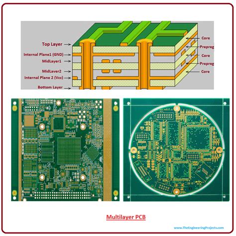
What are Multilayer PCBs?
Multilayer PCBs are circuit boards that consist of three or more conductive copper layers separated by insulating dielectric layers. These layers are laminated together under heat and pressure to form a single board. The conductive layers are interconnected through small holes called vias, which allow signals to pass from one layer to another.
Multilayer PCBs offer several advantages over single or double-sided boards:
- Increased circuit density: With more layers available, designers can pack more components and traces into a smaller area.
- Improved signal integrity: By separating signal layers with ground and power planes, multilayer PCBs can reduce electromagnetic interference (EMI) and crosstalk between signals.
- Better thermal management: The increased number of layers allows for better heat dissipation, which is crucial for high-power applications.
- Enhanced mechanical stability: The laminated structure of multilayer PCBs provides greater rigidity and durability compared to single or double-sided boards.
Factors Affecting the Number of PCB Layers
Determining the optimal number of layers for a multilayer PCB involves considering several factors:
1. Circuit Complexity
The complexity of the electronic circuit is one of the primary factors that influence the number of layers required. As the number of components and interconnections increases, so does the need for additional layers to accommodate them. Complex designs with high component density, such as those found in smartphones or laptops, often require 8 or more layers.
2. Signal Integrity
Maintaining signal integrity is crucial in high-speed digital circuits. As the frequency of signals increases, the risk of signal degradation due to EMI, crosstalk, and other factors also increases. By using dedicated signal layers separated by ground and power planes, designers can minimize these issues. The number of layers required for optimal signal integrity depends on the frequency and sensitivity of the signals involved.
3. Power Distribution
Efficient power distribution is another important consideration in multilayer PCB design. Dedicated power planes help to provide a low-impedance path for power delivery to components, minimizing voltage drops and ensuring stable operation. The number of power planes required depends on the power requirements of the components and the overall system.
4. Cost and Manufacturing Constraints
Increasing the number of layers in a PCB also increases its manufacturing cost. Each additional layer requires more materials, processing steps, and time to produce. Therefore, designers must balance the benefits of additional layers against the increased cost and complexity of manufacturing. Some manufacturing processes may also have limitations on the maximum number of layers that can be produced reliably.

Determining the Number of Layers
To determine the appropriate number of layers for a multilayer PCB, designers typically follow these steps:
-
Assess the circuit complexity: Identify the number of components, their interconnections, and any special requirements such as high-speed signals or power-hungry devices.
-
Create a preliminary layout: Develop an initial component placement and routing scheme to estimate the required board area and layer count.
-
Evaluate signal integrity: Analyze the signal paths and identify any potential issues with EMI, crosstalk, or impedance matching. Determine if additional layers are needed for proper signal isolation and shielding.
-
Consider power distribution: Assess the power requirements of the components and plan for the appropriate number of power planes to ensure stable and efficient power delivery.
-
Optimize the layer stack-up: Arrange the layers to minimize the overall thickness of the board while ensuring proper signal integrity and power distribution. This may involve adjusting the number and placement of signal, ground, and power layers.
-
Evaluate cost and manufacturing constraints: Consider the impact of the layer count on the manufacturing cost and any limitations imposed by the chosen fabrication process. Make adjustments as necessary to balance performance, reliability, and cost.
Here’s an example of a typical layer stack-up for an 8-layer PCB:
| Layer | Type | Description |
|---|---|---|
| 1 | Signal | Top layer for component placement and routing |
| 2 | Ground | Ground plane for signal return and shielding |
| 3 | Signal | Inner layer for signal routing |
| 4 | Power | Power plane for power distribution |
| 5 | Signal | Inner layer for signal routing |
| 6 | Ground | Ground plane for signal return and shielding |
| 7 | Signal | Inner layer for signal routing |
| 8 | Signal | Bottom layer for component placement and routing |
In this example, the signal layers are separated by ground and power planes to minimize EMI and crosstalk. The number of signal layers is balanced against the number of ground and power planes to ensure proper signal integrity and power distribution while minimizing the overall thickness of the board.

Tips for Optimizing PCB Layer Count
Here are some additional tips to help optimize the number of layers in your multilayer PCB design:
-
Use blind and buried vias: These specialized vias connect only the layers they need to, reducing the overall layer count and improving signal integrity.
-
Employ high-density interconnect (HDI) techniques: HDI PCBs use smaller vias and finer traces to increase circuit density without adding more layers.
-
Minimize component count: Whenever possible, use integrated circuits that combine multiple functions to reduce the overall component count and simplify the layout.
-
Use multi-layer PCB design software: Modern PCB design tools have features that help optimize layer stack-up, analyze signal integrity, and estimate manufacturing costs.
-
Collaborate with your PCB manufacturer: Consult with your PCB fabricator early in the design process to ensure that your layer stack-up and design choices are compatible with their manufacturing capabilities.

Frequently Asked Questions (FAQ)
- What is the minimum number of layers in a multilayer PCB?
-
The minimum number of layers in a multilayer PCB is three, consisting of two signal layers and one power or ground layer.
-
How much does each additional layer increase the cost of a PCB?
-
The cost increase per additional layer varies depending on the manufacturer and the specific project requirements. However, a rough estimate is that each additional layer increases the cost by 20-30% compared to the previous layer count.
-
Can I mix different layer types in a multilayer PCB?
-
Yes, it is common to mix signal, ground, and power layers in a multilayer PCB to achieve the desired performance and functionality. The specific arrangement of these layers is called the layer stack-up.
-
What are the limitations on the maximum number of layers in a PCB?
-
The maximum number of layers in a PCB is limited by the manufacturing capabilities of the PCB fabricator. Most manufacturers can produce PCBs with up to 16 layers, while some specialized facilities can handle up to 40 or more layers.
-
How does the number of layers affect the thickness of a PCB?
- The thickness of a PCB increases with the number of layers. Each additional layer adds to the overall thickness of the board, typically by 0.1-0.2mm per layer, depending on the materials used. Designers must consider the thickness constraints of their application when determining the appropriate number of layers.
Conclusion
Determining the optimal number of layers for a multilayer PCB is a critical aspect of electronic design. By carefully considering factors such as circuit complexity, signal integrity, power distribution, and manufacturing constraints, designers can create PCBs that meet the performance, reliability, and cost requirements of their applications.
As electronic devices continue to become more complex and compact, the use of multilayer PCBs with higher layer counts will become increasingly common. By understanding the principles and best practices of multilayer PCB design, engineers can create innovative and efficient electronic products that push the boundaries of what is possible.


Leave a Reply