What is the DRC-Kicad-Issue?
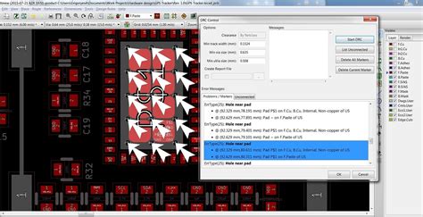
The Design Rule Check (DRC) is an essential tool in PCB design software like Kicad that helps identify potential issues and errors in a PCB Layout before sending it off for manufacturing. One common issue that can arise when running DRC checks in Kicad is with the ground plane copper pour.
The ground plane is a large area of copper, usually on the bottom layer of the PCB, that provides a low-impedance return path for currents and helps reduce EMI. However, if not set up properly, the ground plane can trigger DRC errors that prevent the design from passing validation checks.
Common DRC Errors Related to Ground Planes
Here are some of the most frequently encountered DRC errors when working with ground planes in Kicad:
Clearance Errors
Clearance errors occur when the distance between the ground plane and other traces, pads, or vias is less than the specified clearance rule. This can lead to short circuits or signal integrity issues.
Example clearance rule in Kicad:
| Parameter | Value |
|---|---|
| Pad to pad | 0.2 mm |
| Pad to track | 0.2 mm |
| Track to track | 0.2 mm |
| Via to track | 0.2 mm |
If the ground plane violates any of these clearances, a DRC error will be generated.
Copper to Edge Clearance
This error happens when the ground plane extends too close to the edge of the board outline. PCB Manufacturers require a minimum clearance between copper and the board edge to prevent shortages during fabrication.
Typical edge clearance values:
| Board Thickness | Minimum Clearance |
|---|---|
| <1.0 mm | 0.2 mm |
| 1.0-1.6 mm | 0.3 mm |
| 1.6-3.2 mm | 0.4 mm |
| >3.2 mm | 0.5 mm |
Ensuring the ground plane respects these clearances will avoid DRC errors.
Isolated Copper
Isolated copper errors occur when there are small, unconnected areas of the ground plane that are not attached to the main ground net. These “islands” can cause EMI issues and should be avoided.
Kicad has a “Remove dead copper” option in the copper pour properties that can help eliminate isolated copper areas:
| Option | Recommended Setting |
|---|---|
| Remove dead copper | Checked |
| Thermal relief connect | Reliefs in zones |
| Spoke width | 0.2 mm |
Enabling these options ensures a cleaner ground plane without isolated copper.

Solving Ground Plane DRC Issues
When encountering DRC errors related to the ground plane, here are some steps to troubleshoot and resolve the issues:
-
Review the specific error message and location in the DRC report. This will help pinpoint where the violation is occurring.
-
Check the clearance and edge clearance rules in the Kicad PCB rules settings. Make sure they match your PCB manufacturer’s specifications.
-
Inspect the ground plane copper pour settings. Verify that “Remove dead copper” is enabled and thermal relief connect options are set appropriately.
-
Regenerate the ground plane pour by pressing “B” and selecting the ground net. This will redraw the copper pour and remove any isolated islands.
-
Run the DRC check again to see if the errors have been resolved. If not, repeat steps 1-4 until the design passes all checks.
In some cases, manual editing of the ground plane may be necessary. This can be done using the zone editing tools in Kicad’s PCB editor.

Best Practices for Working with Ground Planes
To minimize the occurrence of ground plane DRC errors, follow these best practices:
-
Set up appropriate clearance and edge clearance rules early in the design process. Consult with your PCB manufacturer for recommended values.
-
Use copper pours for the ground plane instead of manually drawing polygons. This allows for easier modification and regeneration of the plane.
-
Enable “Remove dead copper” and thermal relief connect options in the copper pour settings to avoid isolated copper areas.
-
Run DRC checks regularly during the layout process to catch any issues early on.
-
If manual editing of the ground plane is required, use the zone editing tools and be mindful of clearance rules.
By adhering to these guidelines, designers can create robust and error-free ground planes that pass DRC checks and ensure a successful PCB Fabrication process.

FAQ
- What is the purpose of a ground plane in PCB design?
A ground plane serves several important functions in PCB design:
– Provides a low-impedance return path for currents
– Helps reduce electromagnetic interference (EMI)
– Improves signal integrity by minimizing crosstalk and reflections
– Acts as a heat sink to dissipate thermal energy
- Why is it important to resolve ground plane DRC errors?
Resolving ground plane DRC errors is crucial because:
– Errors can lead to short circuits or signal integrity issues
– PCB manufacturers may reject designs that don’t pass DRC checks
– Unresolved issues can result in non-functional or unreliable boards
– Catching and fixing errors early saves time and money in the long run
- What are some common causes of ground plane DRC errors?
Common causes of ground plane DRC errors include:
– Insufficient clearance between the plane and other traces, pads, or vias
– Ground plane extending too close to the board edge
– Isolated copper areas not connected to the main ground net
– Incorrect copper pour settings in the PCB design software
- How can I prevent ground plane DRC errors in my designs?
To prevent ground plane DRC errors:
– Set up appropriate clearance and edge clearance rules based on manufacturer specs
– Use copper pours with “Remove dead copper” and thermal relief options enabled
– Run DRC checks frequently during the layout process
– Follow best practices for ground plane design and manual editing if needed
- What should I do if I encounter a ground plane DRC error that I can’t resolve?
If you encounter a persistent ground plane DRC error:
– Double-check all clearance and copper pour settings
– Consult with more experienced PCB designers or online forums for advice
– Contact your PCB manufacturer for guidance on their specific DRC requirements
– Consider using alternative layout techniques or redesigning the affected area
By understanding the common issues related to ground planes and following best practices, PCB designers can create robust, error-free layouts that pass DRC checks and ensure successful manufacturing outcomes. Regular use of the DRC tool and attention to detail during the layout process are key to avoiding and resolving ground plane errors in Kicad.


Leave a Reply