Introduction to PCB Stack-up
Printed Circuit Board (PCB) stack-up refers to the arrangement of copper layers and insulating materials that make up a PCB. It is a critical aspect of PCB design, as it determines the board’s electrical properties, signal integrity, and manufacturability. In this article, we will focus on the basic stack-up of a 16-layer PCB board, exploring its components, benefits, and design considerations.
Understanding the Layers in a 16 Layer PCB Stack-up
A 16-layer PCB consists of the following layers:
- Top Layer (Signal)
- Ground Plane
- Signal Layer
- Signal Layer
- Ground Plane
- Signal Layer
- Signal Layer
- Power Plane
- Signal Layer
- Signal Layer
- Ground Plane
- Signal Layer
- Signal Layer
- Ground Plane
- Signal Layer
- Bottom Layer (Signal)
The arrangement of these layers is crucial for ensuring proper signal integrity and minimizing electromagnetic interference (EMI).
Signal Layers
Signal layers are used for routing traces that carry electrical signals between components on the PCB. In a 16-layer PCB, there are typically 10 signal layers (1, 3, 4, 6, 7, 9, 10, 12, 13, and 15). These layers are strategically placed to minimize crosstalk and maintain signal integrity.
Ground Planes
Ground planes (layers 2, 5, 11, and 14) are solid copper layers connected to the ground potential of the circuit. They serve several purposes:
- Providing a low-impedance return path for electrical currents
- Shielding sensitive signals from EMI
- Helping to dissipate heat generated by components
Power Planes
Power planes (layer 8) are solid copper layers that distribute power to components on the PCB. They are typically placed near the center of the stack-up to minimize voltage drop and ensure stable power delivery.

Benefits of a 16 Layer PCB Stack-up
Using a 16-layer PCB stack-up offers several advantages:
-
High Density: With 16 layers, designers can route a large number of traces and accommodate complex circuitry in a compact space.
-
Improved Signal Integrity: The strategic placement of signal, ground, and power layers helps maintain signal integrity by reducing crosstalk and EMI.
-
Enhanced Power Distribution: The dedicated power plane ensures stable and efficient power delivery to all components on the board.
-
Better Thermal Management: The multiple ground planes help dissipate heat generated by components, improving the overall thermal performance of the PCB.

Designing a 16 Layer PCB Stack-up
When designing a 16-layer PCB stack-up, consider the following factors:
Material Selection
Choose appropriate materials for the PCB substrate and insulating layers. Common materials include FR-4, Rogers, and Isola. Consider the dielectric constant, dissipation factor, and thermal properties of the materials based on your application requirements.
Layer Thickness
Determine the thickness of each layer in the stack-up. Typical thicknesses for copper layers range from 0.5 oz to 2 oz, while insulating layers can vary from 2 mil to 8 mil. The overall thickness of the PCB will depend on the number of layers and the chosen material thicknesses.
Impedance Control
Ensure proper impedance control by selecting appropriate trace widths and spacing based on the target impedance and the dielectric properties of the insulating materials. Use impedance calculators or simulation tools to optimize the design.
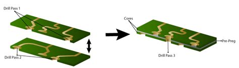
Via Management
Plan the placement and routing of vias to minimize signal degradation and EMI. Use appropriate via types (through-hole, blind, or buried) and sizes based on the signal requirements and manufacturing capabilities.

Example 16 Layer PCB Stack-up
Here’s an example of a 16-layer PCB stack-up with a total thickness of 0.093 inches:
| Layer | Material | Thickness (mil) | Copper Weight (oz) |
|---|---|---|---|
| 1 | FR-4 | 1.2 | 1 |
| 2 | FR-4 | 3.6 | 1 |
| 3 | FR-4 | 1.2 | 1 |
| 4 | FR-4 | 3.6 | 1 |
| 5 | FR-4 | 1.2 | 1 |
| 6 | FR-4 | 3.6 | 1 |
| 7 | FR-4 | 1.2 | 1 |
| 8 | FR-4 | 3.6 | 1 |
| 9 | FR-4 | 1.2 | 1 |
| 10 | FR-4 | 3.6 | 1 |
| 11 | FR-4 | 1.2 | 1 |
| 12 | FR-4 | 3.6 | 1 |
| 13 | FR-4 | 1.2 | 1 |
| 14 | FR-4 | 3.6 | 1 |
| 15 | FR-4 | 1.2 | 1 |
| 16 | FR-4 | 1.2 | 1 |
In this example, the stack-up uses FR-4 material for all layers, with a dielectric constant (Dk) of 4.5 and a dissipation factor (Df) of 0.02. The copper weight for all layers is 1 oz, and the total thickness of the PCB is 0.093 inches (93 mil).
FAQ
1. What is the purpose of a 16-layer PCB stack-up?
A 16-layer PCB stack-up is used for complex designs that require a high number of interconnections and routing density. It allows for the integration of multiple signal, ground, and power layers to ensure proper signal integrity, EMI reduction, and stable power delivery.
2. Can I use different materials for different layers in a 16-layer PCB stack-up?
Yes, you can use different materials for different layers in a 16-layer PCB stack-up. For example, you might use a low-loss material like Rogers for high-speed signal layers and FR-4 for other layers. However, keep in mind that using multiple materials can increase the complexity and cost of the manufacturing process.
3. How does the placement of ground and power planes affect signal integrity?
The placement of ground and power planes plays a crucial role in maintaining signal integrity. Ground planes provide a low-impedance return path for currents and help shield sensitive signals from EMI. Power planes ensure stable power delivery to components and minimize voltage drop. By strategically placing these planes between signal layers, you can reduce crosstalk and improve overall signal quality.
4. What are the challenges in manufacturing a 16-layer PCB?
Manufacturing a 16-layer PCB can be challenging due to several factors:
– Ensuring proper alignment and registration of all layers during the lamination process
– Maintaining consistent dielectric thickness and copper distribution across the board
– Achieving reliable via formation and plating, especially for high aspect ratio vias
– Handling and processing the increased thickness of the PCB
Manufacturers must have advanced equipment, skilled personnel, and strict quality control measures to produce high-quality 16-layer PCBs.
5. How can I optimize the cost of a 16-layer PCB?
To optimize the cost of a 16-layer PCB, consider the following:
– Use standard materials and thicknesses whenever possible
– Minimize the use of blind and buried vias, as they increase manufacturing complexity and cost
– Optimize the PCB layout to reduce the overall board size and layer count, if feasible
– Work closely with your PCB manufacturer to identify cost-saving opportunities in the design and manufacturing process
– Consider alternative stack-up configurations or layer counts that may meet your requirements at a lower cost
Conclusion
A 16-layer PCB stack-up is a complex arrangement of signal, ground, and power layers that enables the design of high-density, high-performance electronic systems. By understanding the basic structure and design considerations of a 16-layer PCB stack-up, engineers can create reliable and efficient PCBs for demanding applications.
When designing a 16-layer PCB, it is essential to carefully select materials, control layer thicknesses, ensure proper impedance control, and manage via placement and routing. Collaborating closely with experienced PCB manufacturers and following best design practices can help optimize the performance, reliability, and cost of the final product.
As technology continues to advance, the use of 16-layer PCBs and beyond will become increasingly common in various industries, from telecommunications and automotive to aerospace and defense. Mastering the art of PCB stack-up design will be crucial for engineers to stay ahead of the curve and deliver cutting-edge electronic solutions.


Leave a Reply