What Are Single-Layer PCBs?
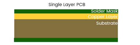
A single-layer PCB, also known as a single-sided PCB, is a printed circuit board that has conductive traces on only one side of the insulating substrate. The conductive traces are usually made of copper and are used to connect various electronic components, such as resistors, capacitors, and integrated circuits (ICs). The insulating substrate is typically made of a material called FR-4, which is a glass-reinforced epoxy laminate.
Advantages of Single-Layer PCBs
- Cost-effective: Single-layer PCBs are the most affordable type of PCB due to their simple design and manufacturing process.
- Easy to design: The single-sided nature of these PCBs makes them easier to design compared to multi-layer PCBs.
- Quick turnaround time: The manufacturing process for single-layer PCBs is relatively simple, resulting in shorter lead times.
- Suitable for low-density designs: Single-layer PCBs are ideal for circuits with a low component density and simple routing requirements.
Disadvantages of Single-Layer PCBs
- Limited routing options: With only one layer available for routing, single-layer PCBs may require jumper wires to complete connections, which can increase the risk of errors and decrease reliability.
- Lower component density: Single-layer PCBs have limited space for components, making them unsuitable for complex designs with high component density.
- Potential for electromagnetic interference (EMI): The lack of a ground plane on single-layer PCBs can lead to increased EMI, which may affect the performance of sensitive electronic components.
Manufacturing Process of Single-Layer PCBs
The manufacturing process for single-layer PCBs involves several steps:
- Designing the PCB layout using electronic design automation (EDA) software.
- Printing the PCB design onto a photosensitive film or directly onto the copper-clad substrate using a laser printer.
- Applying a photoresist layer to the copper-clad substrate and exposing it to UV light through the printed film or direct laser imaging.
- Developing the photoresist to remove the unexposed areas, leaving behind a protective layer in the shape of the PCB design.
- Etching away the unwanted copper using a chemical solution, typically ferric chloride or ammonium persulfate.
- Removing the remaining photoresist layer to reveal the final copper traces.
- Drilling any necessary holes for through-hole components or vias.
- Applying a solder mask to protect the copper traces and prevent short circuits.
- Adding silkscreen labels for component placement and identification.

Applications of Single-Layer PCBs
Single-layer PCBs find applications in various electronic devices and industries, such as:
- Consumer electronics: Remote controls, calculators, and simple electronic toys.
- Automotive industry: Basic control modules and sensors.
- Industrial control systems: Simple control panels and relay boards.
- Prototyping and hobbyist projects: Single-layer PCBs are often used for initial prototypes and small-scale projects due to their affordability and quick turnaround time.

Designing Single-Layer PCBs
When designing single-layer PCBs, there are several key considerations to keep in mind:
- Component placement: Arrange components in a logical manner to minimize the complexity of routing and reduce the need for jumper wires.
- Trace width and spacing: Ensure that the trace width is sufficient to carry the required current and that the spacing between traces is adequate to prevent short circuits.
- Routing techniques: Use efficient routing techniques, such as 45-degree angles and avoiding sharp corners, to minimize signal reflections and improve signal integrity.
- Grounding: Although single-layer PCBs do not have a dedicated ground plane, it is essential to provide a low-impedance path for return currents to minimize EMI and ensure proper circuit functionality.

Comparing Single-Layer PCBs with Other PCB Types
Single-layer PCBs are just one of several types of printed circuit boards available. Here’s a comparison of single-layer PCBs with other common PCB types:
| PCB Type | Layers | Cost | Complexity | Density |
|---|---|---|---|---|
| Single-layer | 1 | Low | Low | Low |
| Double-layer | 2 | Medium | Medium | Medium |
| Multi-layer | 3+ | High | High | High |
| Flexible | Varies | High | High | Medium |
| Rigid-flex | Varies | Very high | Very high | High |
As evident from the table, single-layer PCBs offer the lowest cost and complexity but also have limitations in terms of routing options and component density. Double-layer and multi-layer PCBs provide more flexibility and higher density but come at a higher cost and complexity. Flexible and rigid-Flex PCBs offer unique advantages for specific applications but are more expensive and complex to manufacture.
Single-Layer PCB Design and Assembly Services
Many PCB manufacturing companies offer single-layer PCB design and assembly services to help customers bring their ideas to life. These services typically include:
- PCB design assistance: Some manufacturers provide guidance and support in creating PCB layouts, component selection, and design optimization.
- Prototyping: Quick-turn prototyping services allow customers to test and validate their designs before committing to a full production run.
- Assembly: PCB Assembly services include component sourcing, placement, and soldering, taking the burden off the customer and ensuring a high-quality final product.
When selecting a single-layer PCB design and assembly service provider, consider factors such as experience, capabilities, turnaround time, and customer support to ensure the best possible outcome for your project.
Frequently Asked Questions (FAQ)
- What is the typical thickness of a single-layer PCB?
-
The standard thickness of a single-layer PCB is 1.6 mm (0.063 inches), although thinner and thicker options are available depending on the specific application and manufacturing capabilities.
-
Can single-layer PCBs be used for high-frequency applications?
-
Single-layer PCBs are generally not recommended for high-frequency applications due to their lack of a dedicated ground plane and potential for increased EMI. Double-layer or multi-layer PCBs with proper grounding and shielding are better suited for high-frequency designs.
-
Are single-layer PCBs suitable for automated assembly processes?
-
Yes, single-layer PCBs can be used in automated assembly processes, such as pick-and-place machines and wave soldering. However, the limited routing options and potential for jumper wires may require additional manual intervention compared to more complex PCB types.
-
How do I choose the right copper thickness for my single-layer PCB?
-
The copper thickness, or weight, is typically specified in ounces per square foot (oz/ft²). Common copper weights for single-layer PCBs are 1 oz/ft² and 2 oz/ft², with higher weights providing better current-carrying capacity and lower resistance. The choice of copper weight depends on the specific requirements of your design, such as current demand and trace width.
-
Can single-layer PCBs be used for surface mount technology (SMT) components?
- Yes, single-layer PCBs can accommodate SMT components. However, the limited routing options may require careful component placement and creative routing techniques to ensure proper connections and avoid signal integrity issues.
Conclusion
Single-layer PCBs are a cost-effective and simple solution for a wide range of electronic applications. Despite their limitations in terms of routing options and component density, single-layer PCBs remain a popular choice for simple circuits, prototypes, and low-volume production runs. By understanding the advantages, disadvantages, manufacturing process, and design considerations of single-layer PCBs, engineers and hobbyists can make informed decisions when selecting the appropriate PCB type for their projects.
As the electronics industry continues to evolve, single-layer PCBs will likely remain a valuable tool in the designer’s arsenal, particularly for low-complexity and budget-constrained applications. By leveraging the expertise of experienced PCB design and assembly service providers, customers can bring their single-layer PCB projects to life quickly and efficiently, enabling them to focus on innovation and product development.


Leave a Reply