Introduction to Copper PCBs
Copper Printed Circuit Boards (PCBs) are the backbone of modern electronics. These essential components are found in virtually every electronic device, from smartphones and computers to medical equipment and aerospace systems. Copper PCBs provide a reliable and efficient means of connecting electronic components, allowing for the creation of complex circuits in a compact and organized manner.
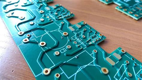
What are Copper PCBs?
Copper PCBs are printed circuit boards that use copper as the primary conductive material for the traces and pads. The copper layer is typically laminated onto a non-conductive substrate, such as FR-4 (a fiberglass-reinforced epoxy resin), which provides mechanical support and insulation between the conductive layers.
Advantages of Copper PCBs
Copper is an ideal material for PCBs due to its excellent electrical conductivity, thermal conductivity, and resistance to corrosion. Some of the key advantages of using copper in PCBs include:
- High electrical conductivity: Copper has one of the highest electrical conductivities among metals, ensuring efficient signal transmission and minimal power loss.
- Thermal conductivity: Copper’s high thermal conductivity helps dissipate heat generated by electronic components, improving the overall reliability and lifespan of the PCB.
- Corrosion resistance: Copper is resistant to corrosion, which helps maintain the integrity of the PCB traces and pads over time.
- Cost-effectiveness: Copper is relatively abundant and affordable compared to other conductive materials, making it a cost-effective choice for PCB manufacturing.
Copper PCB Manufacturing Process
The manufacturing process for copper PCBs involves several key steps, each of which plays a crucial role in ensuring the quality and reliability of the final product.
1. PCB Design and Layout
The first step in the copper PCB manufacturing process is designing the circuit and creating the PCB layout. This involves using specialized software to create a schematic diagram of the circuit and then translating that schematic into a physical layout of the PCB. The layout determines the placement of components, traces, and vias on the board.
2. Substrate Preparation
Once the PCB layout is finalized, the next step is to prepare the substrate. The most common substrate material for copper PCBs is FR-4, a fiberglass-reinforced epoxy resin. The substrate is cut to the desired size and shape, and any necessary holes are drilled for through-hole components and vias.
3. Copper Lamination
The prepared substrate is then laminated with a thin layer of copper on one or both sides, depending on the design requirements. The copper foil is typically 1/2 oz to 2 oz in thickness (17 to 70 µm) and is bonded to the substrate using heat and pressure.
4. Photoresist Application and Exposure
A photoresist layer is applied to the copper surface and then exposed to UV light through a photomask containing the PCB layout pattern. The exposed areas of the photoresist become soluble and can be removed during the development process.
5. Etching
After the photoresist is developed, the exposed copper areas are etched away using a chemical solution, typically ferric chloride or ammonium persulfate. This leaves behind the desired copper traces and pads as defined by the PCB layout.
6. Soldermask and Silkscreen Application
A soldermask layer is applied to the PCB to protect the copper traces and prevent solder bridges during the assembly process. The soldermask is typically green, but other colors are available. A silkscreen layer is then added to provide labels, logos, and other markings on the PCB surface.
7. Surface Finish
The exposed copper areas, such as pads and through-holes, are coated with a surface finish to protect the copper from oxidation and improve solderability. Common surface finishes include HASL (Hot Air Solder Leveling), ENIG (Electroless Nickel Immersion Gold), and OSP (Organic Solderability Preservative).
8. Electrical Testing and Inspection
The completed PCBs undergo thorough electrical testing and visual inspection to ensure they meet the specified design requirements and are free of defects. This may include automated optical inspection (AOI), X-ray inspection, and electrical continuity testing.

Types of Copper PCBs
Copper PCBs can be categorized based on various factors, such as the number of layers, the type of copper used, and the specific manufacturing processes employed.
Single-layer vs. Multi-layer PCBs
Single-layer PCBs have copper traces on only one side of the substrate, while multi-layer PCBs have copper traces on both sides and may also have internal copper layers. Multi-layer PCBs offer higher component density and better signal integrity compared to single-layer PCBs.
Standard Copper vs. Heavy Copper PCBs
Standard copper PCBs use copper foil with a thickness of 1/2 oz to 2 oz (17 to 70 µm), which is suitable for most applications. Heavy copper PCBs, on the other hand, use copper foil with a thickness of 3 oz or more (105 µm or thicker). Heavy copper PCBs are used in high-power applications, such as power electronics and automotive systems, where higher current-carrying capacity is required.
Rigid vs. Flexible PCBs
Rigid PCBs are made with a solid substrate, such as FR-4, and are used in most electronic devices. Flexible PCBs (FPCBs) use a flexible substrate, such as polyimide or polyester, and can be bent or folded to fit into tight spaces or conform to unique shapes. FPCBs are commonly used in wearable electronics, medical devices, and aerospace applications.

Copper PCB Fabricators and Manufacturers
There are numerous copper PCB fabricators and manufacturers worldwide, each with their own specialties and capabilities. Some of the key factors to consider when choosing a copper PCB manufacturer include:
- Manufacturing capabilities: Ensure the manufacturer can produce PCBs that meet your specific requirements, such as layer count, copper thickness, and surface finish.
- Quality control: Look for manufacturers with robust quality control processes and certifications, such as ISO 9001, IATF 16949, or IPC standards.
- Lead times: Consider the manufacturer’s lead times and whether they can meet your production schedule.
- Cost: Compare pricing from multiple manufacturers, but be cautious of sacrificing quality for lower costs.
- Customer support: Choose a manufacturer with responsive and knowledgeable customer support to help address any issues that may arise during the manufacturing process.
Some notable copper PCB fabricators and manufacturers include:
| Company | Location | Specialties |
|---|---|---|
| Kinwong Electronic | China | High-volume production, Automotive PCBs |
| Nippon Mektron | Japan | Flexible PCBs, high-density interconnects |
| SEMCO (Samsung Electro-Mechanics) | South Korea | Multi-layer PCBs, package substrates |
| TTM Technologies | United States | Aerospace and defense PCBs, RF/microwave PCBs |
| Unimicron | Taiwan | HDI PCBs, IC substrates |

Future Trends in Copper PCB Manufacturing
As electronic devices continue to become smaller, more powerful, and more interconnected, copper PCB manufacturing technologies must evolve to keep pace with these trends. Some of the key future trends in copper PCB manufacturing include:
Miniaturization and Increased Density
The demand for smaller and more compact electronic devices is driving the need for PCBs with higher component density and finer trace widths and spacing. Advanced manufacturing techniques, such as modified semi-additive process (mSAP) and embedded component technology, are enabling the production of ultra-high-density interconnects (UHDI) and miniaturized PCBs.
5G and High-Frequency Applications
The rollout of 5G networks and the increasing use of high-frequency technologies, such as millimeter-wave (mmWave) and terahertz (THz) frequencies, require PCBs with improved signal integrity and low-loss characteristics. Copper PCB manufacturers are developing new materials and processes to meet these challenges, such as low-loss substrates and advanced surface finishes.
Sustainability and Environmental Concerns
As environmental regulations become more stringent, copper PCB manufacturers are adopting more sustainable and eco-friendly practices. This includes the use of halogen-free and lead-free materials, as well as the implementation of green manufacturing processes that reduce waste and energy consumption.
Industry 4.0 and Smart Manufacturing
The integration of Industry 4.0 technologies, such as artificial intelligence (AI), machine learning (ML), and the Internet of Things (IoT), is transforming the copper PCB manufacturing landscape. Smart factories with automated and interconnected production systems are enabling faster, more efficient, and more flexible manufacturing processes, while also improving quality control and reducing costs.
Frequently Asked Questions (FAQs)
-
What is the difference between copper PCBs and Aluminum PCBs?
Copper PCBs use copper as the primary conductive material, while aluminum PCBs use aluminum. Copper is more commonly used due to its superior electrical and thermal conductivity, as well as its better resistance to corrosion. Aluminum PCBs are sometimes used in specific applications where weight reduction is a priority. -
Can copper PCBs be recycled?
Yes, copper PCBs can be recycled. The recycling process typically involves shredding the PCBs and then separating the copper from the other materials using various techniques, such as density separation, electrostatic separation, and chemical processing. Recycling copper from PCBs helps reduce electronic waste and conserves natural resources. -
What is the minimum trace width and spacing for copper PCBs?
The minimum trace width and spacing for copper PCBs depend on the specific manufacturing capabilities of the fabricator and the chosen copper thickness. For standard 1 oz copper, the minimum trace width and spacing is typically around 100 µm (4 mil). With advanced manufacturing techniques, such as mSAP, trace widths and spacing can be reduced to 50 µm (2 mil) or less. -
How do I choose the right copper thickness for my PCB?
The choice of copper thickness depends on the specific electrical and thermal requirements of your application. Thicker copper layers can carry more current and provide better heat dissipation, but they also increase the overall thickness and weight of the PCB. For most applications, 1 oz copper (35 µm) is sufficient. However, for high-power applications, 2 oz (70 µm) or heavy copper (3 oz/105 µm or thicker) may be necessary. -
What is the typical lead time for copper PCB manufacturing?
The lead time for copper PCB manufacturing varies depending on the complexity of the design, the chosen manufacturer, and the order quantity. For standard PCBs, lead times can range from a few days to a few weeks. For more complex designs or large order quantities, lead times can extend to several weeks or even months. It’s essential to discuss lead times with your chosen manufacturer and plan accordingly to ensure timely delivery of your PCBs.
Conclusion
Copper PCBs are essential components in modern electronics, providing a reliable and efficient means of connecting electronic components in a compact and organized manner. The copper PCB manufacturing process involves several key steps, from design and layout to substrate preparation, copper lamination, etching, and surface finishing. Copper PCBs can be categorized based on various factors, such as the number of layers, copper thickness, and substrate flexibility.
When choosing a copper PCB fabricator or manufacturer, it’s essential to consider factors such as manufacturing capabilities, quality control, lead times, cost, and customer support. As electronic devices continue to evolve, copper PCB manufacturing technologies must also advance to meet the demands for miniaturization, high-frequency applications, sustainability, and smart manufacturing.
By understanding the fundamentals of copper PCBs and staying informed about the latest trends and technologies in PCB manufacturing, engineers and designers can create innovative and reliable electronic products that meet the needs of an increasingly connected and technology-driven world.


Leave a Reply