Understanding the PCB Silkscreen and Its Importance
When it comes to printed circuit boards (PCBs), one essential component that often goes unnoticed is the silkscreen. The PCB silkscreen, also known as the legend or nomenclature, is a layer of text and symbols printed on the surface of the PCB. This layer provides crucial information about the board’s components, orientation, and functionality, making it easier for engineers, technicians, and manufacturers to assemble, test, and debug the PCB.
In this article, we will dive deep into the world of PCB silkscreens, exploring their purpose, design considerations, and best practices for creating effective and informative silkscreens.
Table of Contents
- What is a PCB Silkscreen?
- The Purpose of PCB Silkscreens
- Silkscreen Printing Process
- Silkscreen Design Considerations
- Font and Size
- Placement and Orientation
- Color and Contrast
- Silkscreen Content
- Component Identification
- Polarity and Orientation Indicators
- Test Points and Fiducials
- Branding and Logos
- Silkscreen Best Practices
- FAQ
- Conclusion
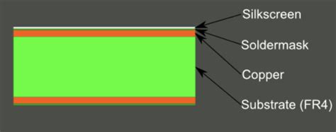
1. What is a PCB Silkscreen?
A PCB silkscreen is a layer of text and symbols printed on the surface of a printed circuit board. The silkscreen layer is typically the topmost layer of the PCB and is applied using a screen printing process. The purpose of the silkscreen is to provide essential information about the board’s components, orientation, and functionality, making it easier for engineers, technicians, and manufacturers to assemble, test, and debug the PCB.

2. The Purpose of PCB Silkscreens
PCB silkscreens serve several important purposes, including:
-
Component Identification: The silkscreen layer is used to label components on the PCB, making it easier for technicians to identify and replace them during assembly or repair.
-
Orientation Guidance: Silkscreens often include orientation indicators, such as pin 1 markers or polarity symbols, to ensure that components are installed correctly.
-
Assembly Instructions: The silkscreen can provide instructions or notes for the assembly process, such as indicating the order in which components should be installed or specifying torque values for screws.
-
Testing and Debugging: Silkscreens can label test points, jumpers, and other features that are important for testing and debugging the PCB.
-
Branding and Aesthetics: Silkscreens can include company logos, product names, or other branding elements to improve the appearance of the PCB and reinforce brand identity.

3. Silkscreen Printing Process
The silkscreen printing process involves the following steps:
-
Artwork Creation: The silkscreen artwork is created using PCB design software, such as Altium Designer or KiCad. The artwork is typically created as a vector image and includes all the text, symbols, and graphics that will be printed on the PCB.
-
Screen Preparation: A fine mesh screen is coated with a light-sensitive emulsion and exposed to UV light through the artwork. The exposed areas of the emulsion harden, while the unexposed areas remain soft and can be washed away, creating a stencil of the artwork on the screen.
-
Ink Application: The screen is placed over the PCB, and ink is applied to the screen using a squeegee. The ink passes through the open areas of the stencil and onto the surface of the PCB.
-
Curing: The printed PCB is then cured, typically using heat or UV light, to ensure that the ink adheres properly to the surface of the board.

4. Silkscreen Design Considerations
When designing a PCB silkscreen, there are several important factors to consider, including:
Font and Size
The font and size of the text on the silkscreen should be legible and consistent. It is recommended to use a sans-serif font, such as Arial or Helvetica, with a minimum size of 0.8mm (0.032 inches) for main text and 0.5mm (0.020 inches) for subscript or superscript characters.
| Text Type | Minimum Size |
|---|---|
| Main Text | 0.8mm (0.032 inches) |
| Subscript/Superscript | 0.5mm (0.020 inches) |
Placement and Orientation
The placement and orientation of the silkscreen elements should be carefully considered to ensure that they are easily readable and do not interfere with other components on the PCB. It is important to maintain adequate clearance between the silkscreen and other features, such as pads, traces, and vias.
| Feature | Minimum Clearance |
|---|---|
| Pads | 0.2mm (0.008 inches) |
| Traces | 0.15mm (0.006 inches) |
| Vias | 0.2mm (0.008 inches) |
Color and Contrast
The color of the silkscreen should provide good contrast against the background color of the PCB to ensure legibility. White silkscreen on a green or black PCB is the most common combination, but other colors can be used for specific applications or to enhance the appearance of the board.
| PCB Color | Recommended Silkscreen Color |
|---|---|
| Green | White |
| Black | White |
| Blue | White or Yellow |
| Red | White or Black |
5. Silkscreen Content
The content of the silkscreen should be carefully planned to provide all the necessary information without cluttering the PCB. Some of the essential elements that should be included in the silkscreen are:
Component Identification
Each component on the PCB should be clearly labeled with its reference designator, such as R1 for resistors, C1 for capacitors, and U1 for integrated circuits. The labels should be placed near the component, preferably on the same side of the board as the component itself.
Polarity and Orientation Indicators
Polarity and orientation indicators, such as pin 1 markers or cathode/anode symbols, should be included to ensure that components are installed correctly. These indicators should be placed consistently and in accordance with industry standards.
Test Points and Fiducials
Test points and fiducials should be clearly labeled on the silkscreen to facilitate testing and automated assembly. Test points can be labeled with their function or a unique identifier, while fiducials should be marked with crosshairs or other standard symbols.
Branding and Logos
Company logos, product names, and other branding elements can be included on the silkscreen to improve the appearance of the PCB and reinforce brand identity. However, it is important to ensure that these elements do not interfere with the functional aspects of the silkscreen.
6. Silkscreen Best Practices
To create effective and informative PCB silkscreens, follow these best practices:
- Keep the silkscreen clean and uncluttered by only including essential information.
- Use a consistent font, size, and style throughout the silkscreen.
- Maintain adequate clearance between the silkscreen and other PCB features.
- Use industry-standard symbols and conventions for polarity, orientation, and test points.
- Ensure good contrast between the silkscreen color and the PCB background color.
- Verify that the silkscreen artwork matches the final PCB layout before fabrication.
- Consider using both top and bottom silkscreens for complex boards or those with components on both sides.
7. FAQ
-
Q: Can silkscreens be used on both sides of the PCB?
A: Yes, silkscreens can be applied to both the top and bottom sides of the PCB. This is particularly useful for complex boards or those with components on both sides. -
Q: Are there any limitations on the colors that can be used for silkscreens?
A: While there are no strict limitations on silkscreen colors, it is essential to choose colors that provide good contrast against the PCB background color. White, black, and yellow are the most commonly used colors. -
Q: Can silkscreens be used for solder masks?
A: No, silkscreens are not used for solder masks. Solder masks are a separate layer that is applied to the PCB to protect the copper traces and prevent solder bridging. -
Q: How durable are silkscreens?
A: Silkscreens are relatively durable and can withstand normal handling and soldering processes. However, they can be damaged by abrasion or exposure to harsh chemicals. -
Q: Can silkscreens be customized with logos or graphics?
A: Yes, silkscreens can include custom logos, graphics, or other branding elements. However, it is important to ensure that these elements do not interfere with the functional aspects of the silkscreen.
8. Conclusion
PCB silkscreens play a crucial role in the assembly, testing, and debugging of printed circuit boards. By providing clear and concise information about components, orientation, and functionality, silkscreens help to streamline the manufacturing process and reduce the likelihood of errors.
When designing PCB silkscreens, it is essential to consider factors such as font, size, placement, color, and content to ensure that the silkscreen is legible, informative, and unobtrusive. By following industry standards and best practices, engineers and designers can create silkscreens that effectively communicate essential information and contribute to the overall quality and reliability of the PCB.
As PCB technology continues to evolve, the importance of well-designed silkscreens will only continue to grow. By understanding the principles and techniques behind effective silkscreen design, engineers and manufacturers can create PCBs that are easier to assemble, test, and maintain, ultimately leading to better products and more satisfied customers.


Leave a Reply