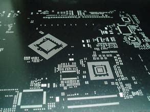
How PCB Stencils Work
PCB stencils work by allowing solder paste to be selectively deposited onto the PCB pads through the openings in the stencil. The stencil is aligned with the PCB, and solder paste is applied using a squeegee or automated printer. The paste is forced through the openings, depositing the correct amount onto each pad. After the stencil is removed, the PCB is ready for component placement.
The key aspects of how PCB stencils work include:
-
Stencil design: The stencil openings must match the size, shape, and location of the PCB pads. Stencil design considerations include aperture size, pitch, and shape, as well as the overall stencil thickness.
-
Alignment: Precise alignment between the stencil and PCB is critical for accurate solder paste deposition. Alignment is typically achieved using fiducial markers or dedicated alignment systems.
-
Solder paste application: The solder paste is applied to the stencil using a squeegee or automated printer. The squeegee moves across the stencil, forcing the paste through the openings and onto the PCB pads.
-
Stencil removal: After the solder paste is applied, the stencil is carefully removed from the PCB. The deposited solder paste should maintain its shape and adhere to the pads.
Benefits of Using PCB Stencils
Using PCB stencils offers several benefits in the SMT assembly process:
-
Consistency: Stencils ensure consistent solder paste volume and placement across the entire PCB, reducing the risk of defects caused by insufficient or excessive solder.
-
Accuracy: Well-designed stencils enable precise solder paste deposition, even for fine-pitch components and high-density layouts.
-
Efficiency: Stencils allow for rapid solder paste application, significantly reducing the time required for manual or semi-automated processes.
-
Cost-effectiveness: By minimizing solder paste waste and reducing rework due to solder defects, stencils contribute to overall cost savings in PCB Assembly.
-
Scalability: Stencils are suitable for high-volume production, enabling consistent results across large batches of PCBs.

Types of PCB Stencils
There are several types of PCB stencils, each with its own characteristics and applications:
Stainless Steel Stencils
Stainless steel stencils are the most common type used in PCB assembly. They offer excellent durability, precision, and compatibility with various solder paste formulations. Stainless steel stencils can be either laser-cut or chemically etched, depending on the required aperture size and shape.
| Stencil Type | Thickness Range | Minimum Aperture Size | Durability |
|---|---|---|---|
| Laser-cut | 0.1 mm – 0.2 mm | 0.1 mm | High |
| Chem-etched | 0.1 mm – 0.3 mm | 0.05 mm | High |
Polyimide Stencils
Polyimide stencils, also known as polymer stencils, are made from a flexible, high-temperature resistant material. They are well-suited for applications requiring conformity to uneven surfaces or for use with flexible PCBs. Polyimide stencils are typically laser-cut and can achieve fine aperture sizes.
| Stencil Type | Thickness Range | Minimum Aperture Size | Compatibility |
|---|---|---|---|
| Polyimide | 0.05 mm – 0.2 mm | 0.05 mm | Flexible PCBs |
Electroformed Stencils
Electroformed stencils, also referred to as nickel stencils, are created through an electroplating process. They offer excellent aperture uniformity and can achieve very fine aperture sizes, making them suitable for high-density PCB layouts and ultra-fine pitch components.
| Stencil Type | Thickness Range | Minimum Aperture Size | Precision |
|---|---|---|---|
| Electroformed | 0.05 mm – 0.15 mm | 0.03 mm | Ultra-high |

Stencil Design Considerations
Proper stencil design is essential for achieving optimal solder paste deposition and ensuring PCB assembly success. Key design considerations include:
-
Aperture size and shape: The size and shape of the stencil apertures should be optimized based on the PCB pad dimensions, component pitch, and solder paste properties. Common aperture shapes include square, circular, and home plate.
-
Stencil thickness: The stencil thickness determines the volume of solder paste deposited. Thicker stencils deposit more paste, while thinner stencils are better suited for fine-pitch components. Typical stencil thicknesses range from 0.1 mm to 0.2 mm.
-
Area ratio: The area ratio is the relationship between the aperture opening and the aperture wall area. A higher area ratio promotes better paste release and reduces the risk of clogging. A minimum area ratio of 0.66 is generally recommended.
-
Overprinting: Overprinting involves extending the stencil aperture beyond the PCB pad to compensate for misalignment or to achieve a specific solder joint profile. Overprinting should be used judiciously to avoid solder bridging.
-
Fiducial marks: Fiducial marks on the stencil and PCB facilitate accurate alignment during the solder paste printing process. At least three fiducial marks should be used for optimal alignment.

Stencil Printing Process
The stencil printing process involves several steps to ensure accurate and consistent solder paste deposition:
-
Stencil and PCB preparation: The stencil and PCB are cleaned to remove any contaminants or debris that could affect the printing process. The stencil is then aligned with the PCB using the fiducial marks.
-
Solder paste loading: Solder paste is applied to the stencil surface, typically using a automated dispenser or manually with a squeegee.
-
Solder paste printing: The squeegee or automated printer moves across the stencil, forcing the solder paste through the apertures and onto the PCB pads. Printer settings such as squeegee pressure, speed, and angle are adjusted to achieve optimal results.
-
Stencil removal: After printing, the stencil is carefully lifted from the PCB, leaving the solder paste deposits on the pads. The PCB is then ready for component placement.
-
Inspection: The printed PCB is inspected to verify the accuracy and consistency of the solder paste deposits. Automated solder paste inspection (SPI) systems can be used to detect defects such as insufficient paste, bridging, or misalignment.
Stencil Maintenance and Cleaning
Proper maintenance and cleaning of PCB stencils are crucial for ensuring consistent performance and prolonging stencil life. Key considerations include:
-
Cleaning frequency: Stencils should be cleaned regularly to remove solder paste residue and prevent clogging of the apertures. The cleaning frequency depends on factors such as paste type, printing volume, and environmental conditions.
-
Cleaning methods: Stencils can be cleaned using various methods, including manual cleaning with solvents, ultrasonic cleaning, and automated stencil cleaners. The choice of cleaning method depends on the stencil material, solder paste, and production requirements.
-
Storage: When not in use, stencils should be stored in a clean, dry environment to prevent damage and contamination. Stencils should be kept in protective containers or racks to minimize the risk of physical damage.
-
Inspection: Regular inspection of the stencil for signs of wear, damage, or clogging is important for maintaining optimal performance. Damaged or worn stencils should be repaired or replaced as necessary.
Frequently Asked Questions (FAQ)
1. What is the difference between a solder paste stencil and a solder mask?
A solder paste stencil is used to apply solder paste onto the PCB pads before component placement, while a solder mask is a protective layer applied to the PCB to prevent solder from adhering to non-pad areas. Solder masks also provide insulation and protection for the PCB traces.
2. Can PCB stencils be reused?
Yes, PCB stencils can be reused multiple times with proper cleaning and maintenance. The number of times a stencil can be reused depends on factors such as the stencil material, solder paste type, and printing conditions.
3. How do I choose the right stencil thickness for my PCB?
The choice of stencil thickness depends on factors such as the component pitch, pad size, and solder paste properties. As a general guideline, use thinner stencils (0.1 mm to 0.15 mm) for fine-pitch components and thicker stencils (0.15 mm to 0.2 mm) for larger components. It is recommended to consult with your stencil supplier or assembly partner for specific guidance.
4. What is the shelf life of a PCB stencil?
The shelf life of a PCB stencil depends on the stencil material and storage conditions. Stainless steel stencils have a virtually unlimited shelf life when stored properly, while polyimide stencils may degrade over time due to exposure to UV light and other environmental factors. It is important to store stencils in a clean, dry environment and inspect them regularly for signs of damage or wear.
5. How do I troubleshoot common solder paste printing issues?
Common solder paste printing issues include insufficient paste deposition, bridging, and misalignment. To troubleshoot these issues, consider the following:
– Check the stencil aperture size and shape for compatibility with the pad dimensions and paste properties.
– Verify the stencil alignment and adjust as necessary.
– Optimize the printer settings, such as squeegee pressure, speed, and angle.
– Ensure proper cleaning and maintenance of the stencil and printing equipment.
– Investigate the solder paste properties and storage conditions for any potential issues.
If the problems persist, consult with your stencil supplier or assembly partner for further assistance.
Conclusion
PCB stencils play a critical role in the SMT assembly process, enabling accurate and consistent solder paste deposition onto PCB pads. By understanding the types of stencils, design considerations, printing process, and maintenance requirements, PCB designers and assembly professionals can optimize their stencil usage for improved PCB Quality and reliability. As PCB technology continues to advance, the importance of precise and efficient solder paste printing will only increase, making PCB stencils an essential tool in the electronics manufacturing industry.


Leave a Reply