Introduction to PCB Fabrication
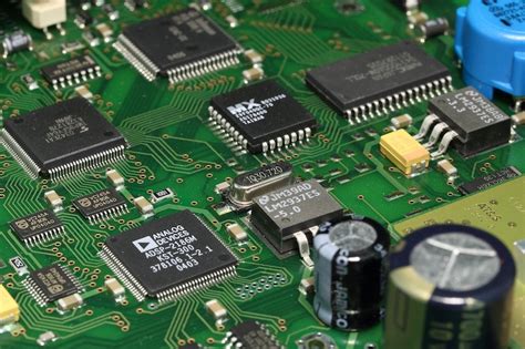
PCB (Printed Circuit Board) fabrication is the process of creating a circuit board that connects electronic components using conductive tracks, pads, and other features. PCBs are essential in modern electronics, as they provide a reliable and efficient way to assemble and connect various components in a compact space. This article aims to answer some of the most common questions about PCB fabrication, covering topics such as the fabrication process, materials, design considerations, and more.
The PCB Fabrication Process
Step 1: PCB Design and Preparation
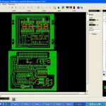
The first step in PCB fabrication is designing the circuit board using specialized software such as Altium Designer, Eagle, or KiCad. The design includes the placement of components, routing of traces, and creation of solder mask and silkscreen layers. Once the design is complete, the files are prepared for manufacturing, which typically includes generating Gerber files and drill files.
Step 2: PCB Material Selection
PCBs are typically made from a substrate material called FR-4, which is a glass-reinforced epoxy laminate. Other materials, such as polyimide or PTFE, may be used for high-frequency or high-temperature applications. The substrate is coated with a thin layer of copper on one or both sides, depending on the design requirements.
Step 3: PCB Etching
The next step is to etch away the unwanted copper from the substrate, leaving only the desired traces and pads. This is done using a photoresist and a chemical etching process. First, the copper-clad substrate is coated with a light-sensitive photoresist. Then, the PCB design is transferred to the photoresist using a photomask and exposure to UV light. The exposed photoresist is then developed, revealing the copper to be etched away. The board is then immersed in an etching solution, typically ferric chloride or ammonium persulfate, which removes the unwanted copper.
Step 4: Drilling and Plating
After etching, the PCB is drilled to create holes for through-hole components and vias. The holes are then plated with copper to create electrical connections between layers. This is done using an electroplating process, where the board is immersed in a copper sulfate solution and an electric current is applied to deposit copper onto the walls of the drilled holes.
Step 5: Solder Mask and Silkscreen Application
A solder mask is a protective layer applied to the PCB to prevent accidental short circuits and protect the copper traces from oxidation. The solder mask is typically green, but other colors are available. The silkscreen layer is used to add text and symbols to the PCB for component identification and assembly instructions. Both the solder mask and silkscreen are applied using a screen printing process.
Step 6: Surface Finish
The final step in PCB fabrication is to apply a surface finish to the exposed copper areas, such as pads and through-holes. The surface finish protects the copper from oxidation and enhances the solderability of the board. Common surface finishes include HASL (Hot Air Solder Leveling), ENIG (Electroless Nickel Immersion Gold), and OSP (Organic Solderability Preservative).
PCB Design Considerations
When designing a PCB, there are several factors to consider to ensure optimal performance and manufacturability. Some of these considerations include:
Component Placement
Proper component placement is crucial for both circuit functionality and assembly. Components should be placed in a logical order, with related components grouped together. Adequate spacing should be maintained between components to allow for proper soldering and to minimize electromagnetic interference (EMI).
Trace Routing
Traces should be routed in a way that minimizes signal interference and maintains signal integrity. This includes using appropriate trace widths, avoiding sharp angles, and maintaining proper spacing between traces. In high-frequency designs, impedance control and differential pair routing become critical considerations.
Power and Ground Planes
Power and ground planes are used to distribute power and provide a low-impedance return path for signals. These planes help to reduce noise and EMI, and they should be designed with proper decoupling and bypass capacitors to ensure stable power delivery.
Thermal Management
Proper thermal management is essential to ensure the reliability and longevity of the PCB and its components. This includes providing adequate copper area for heat dissipation, using thermal vias to transfer heat to other layers, and considering the use of heatsinks or fans for high-power components.

PCB Materials and Specifications
When selecting PCB materials and specifying requirements, several factors should be considered, including:
Material Properties
FR-4 is the most common PCB substrate material, but other materials like polyimide, PTFE, or Rogers laminates may be used for specific applications. The choice of material depends on factors such as the operating temperature range, dielectric constant, loss tangent, and thermal conductivity.
Copper Weight
Copper weight refers to the thickness of the copper layer on the PCB, typically measured in ounces per square foot (oz/ft²). Common copper weights include 0.5 oz/ft², 1 oz/ft², and 2 oz/ft². Thicker copper is used for high-current applications or to improve thermal dissipation.
Board Thickness
PCB thickness is typically specified in mils (thousandths of an inch). Common thicknesses range from 0.031″ (0.8 mm) to 0.125″ (3.2 mm). Thicker boards provide better mechanical stability and thermal dissipation, while thinner boards are used for space-constrained applications.
Minimum Feature Size
The minimum feature size refers to the smallest trace width, spacing, or hole size that can be reliably manufactured. This is determined by the capabilities of the PCB fabrication process and the design rules specified by the manufacturer. Smaller feature sizes allow for denser layouts but may increase manufacturing costs.
Common PCB Types and Applications
PCBs can be classified based on their layer count, component mounting method, and application. Some common types include:
Single-layer PCBs
Single-layer PCBs have components and traces on only one side of the substrate. They are the simplest and most cost-effective type of PCB, suitable for low-complexity designs.
Double-layer PCBs
Double-layer PCBs have components and traces on both sides of the substrate, with plated through-holes connecting the layers. They offer more design flexibility and higher component density than single-layer boards.
Multi-layer PCBs
Multi-layer PCBs have three or more copper layers, with insulating layers separating them. They are used for complex designs that require high component density, signal integrity, and EMI control. The number of layers can range from 4 to over 50 in some high-end applications.
Flexible PCBs
Flexible PCBs are made from flexible substrate materials, such as polyimide or polyester. They can bend and flex, making them suitable for applications with limited space or movable parts, such as mobile devices, wearables, and automotive electronics.
Rigid-Flex PCBs
Rigid-flex PCBs combine rigid and flexible sections in a single board. The rigid sections provide mechanical support and accommodate standard components, while the flexible sections allow for bending and folding. This type of PCB is often used in aerospace, medical, and industrial applications.
PCB Testing and Quality Control
To ensure the reliability and performance of PCBs, various testing and quality control methods are employed during and after the fabrication process. Some common methods include:
Automated Optical Inspection (AOI)
AOI uses cameras and image processing software to inspect the PCB for defects such as missing components, incorrect component placement, or solder bridging. This is a fast and efficient method for detecting visible defects.
X-Ray Inspection
X-ray inspection is used to detect defects that are not visible on the surface, such as voids in solder joints or misaligned ball grid array (BGA) components. This method is particularly useful for inspecting high-density boards with hidden connections.
In-Circuit Testing (ICT)
ICT involves using a bed-of-nails fixture to make electrical contact with specific points on the PCB and verify the proper connectivity and component values. This method can detect short circuits, open circuits, and component failures.
Functional Testing
Functional testing involves powering up the PCB and verifying its operation under real-world conditions. This can be done using custom test fixtures or by integrating the PCB into the final product and performing system-level tests.
Frequently Asked Questions (FAQ)
1. What is the typical turnaround time for PCB fabrication?
The turnaround time for PCB fabrication depends on the complexity of the design, the manufacturing process, and the workload of the fabrication facility. For standard designs, turnaround times can range from 24 hours for quick-turn prototypes to 1-2 weeks for larger production runs. More complex designs or specialty materials may require longer lead times.
2. How much does PCB fabrication cost?
The cost of PCB fabrication depends on several factors, including the board size, layer count, material, surface finish, and quantity. In general, larger quantities and simpler designs result in lower per-unit costs. For small quantities or prototypes, prices can range from a few dollars to several hundred dollars per board, depending on the complexity.
3. What are the most common PCB surface finishes?
The most common PCB surface finishes are:
- HASL (Hot Air Solder Leveling): A tin-lead alloy is applied to the exposed copper surfaces, providing good solderability and low cost.
- ENIG (Electroless Nickel Immersion Gold): A thin layer of nickel is deposited on the copper, followed by a thin layer of gold. This finish provides excellent solderability, corrosion resistance, and shelf life.
- OSP (Organic Solderability Preservative): A thin, clear organic coating is applied to the copper to protect it from oxidation. This finish is low-cost and suitable for quick-turn prototypes.
4. What is the difference between through-hole and surface-mount components?
Through-hole components have leads that are inserted into drilled holes in the PCB and soldered on the opposite side. Surface-mount components are mounted directly onto the surface of the PCB and soldered in place. Surface-mount components are generally smaller and allow for higher component density, while through-hole components are more robust and easier to assemble manually.
5. Can I fabricate a PCB at home?
Yes, it is possible to fabricate simple PCBs at home using methods such as the toner transfer method or by using a CNC mill. However, home fabrication is limited in terms of the achievable complexity, precision, and reliability compared to professional PCB fabrication services. Home fabrication is best suited for simple, low-frequency designs and educational purposes.
Conclusion
PCB fabrication is a complex process that involves multiple steps, materials, and design considerations. Understanding the basics of PCB fabrication, including the manufacturing process, material selection, design guidelines, and testing methods, is essential for creating reliable and high-performance electronic devices. By working with experienced PCB fabrication services and following best practices in design and manufacturing, you can ensure the success of your electronic projects.
| PCB Fabrication Process | Description |
|---|---|
| PCB Design and Preparation | Designing the circuit board using specialized software and preparing files for manufacturing |
| PCB Material Selection | Choosing the appropriate substrate material and copper weight based on design requirements |
| PCB Etching | Removing unwanted copper from the substrate using photoresist and chemical etching |
| Drilling and Plating | Creating holes for components and vias, and plating them with copper for electrical connections |
| Solder Mask and Silkscreen Application | Applying a protective solder mask and adding text and symbols for component identification |
| Surface Finish | Applying a surface finish to exposed copper areas to protect from oxidation and enhance solderability |
| Common PCB Surface Finishes | Description |
|---|---|
| HASL (Hot Air Solder Leveling) | A tin-lead alloy is applied to the exposed copper surfaces, providing good solderability and low cost |
| ENIG (Electroless Nickel Immersion Gold) | A thin layer of nickel is deposited on the copper, followed by a thin layer of gold, providing excellent solderability and corrosion resistance |
| OSP (Organic Solderability Preservative) | A thin, clear organic coating is applied to the copper to protect it from oxidation, suitable for quick-turn prototypes |
As PCB fabrication continues to evolve, new technologies and materials will emerge to meet the ever-increasing demands of the electronics industry. By staying informed about the latest developments in PCB fabrication and maintaining a focus on quality and reliability, designers and manufacturers can create innovative and successful electronic products.
Leave a Reply