What is PCB etching?
PCB etching is the process of selectively removing copper from a printed circuit board (PCB) to create the desired electrical connections between components. The copper is removed using a chemical etching solution, leaving behind the PCB traces that form the circuit.
PCB etching is a crucial step in the PCB fabrication process. It allows for the precise and intricate patterns of copper traces to be created on the PCB substrate. The etched PCB then serves as the foundation for soldering on electronic components to create a functional circuit board.
PCB Etching Methods
There are two main methods for etching PCBs:
-
Ferric Chloride Etching: This is the most common method used by hobbyists and small-scale PCB fabricators. It involves submerging the PCB in a heated ferric chloride solution which etches away the exposed copper.
-
Ammonium Persulfate Etching: This method uses an ammonium persulfate solution instead of ferric chloride. It is less commonly used but offers some advantages such as being reusable and less messy.
For this guide, we will focus on the ferric chloride etching method as it is the most accessible for beginners.

Materials and Tools Needed for PCB Etching
Before starting the PCB etching process, gather the following materials and tools:
| Material/Tool | Purpose |
|---|---|
| Copper clad board | The base material for the PCB |
| Laser printer | For printing the PCB design onto transfer paper |
| Glossy paper or transfer paper | For transferring the PCB design to the copper board |
| Clothes iron | For ironing the design onto the copper board |
| Ferric chloride solution | The chemical etchant for removing copper |
| Plastic container | For holding the ferric chloride solution during etching |
| Rubber gloves and safety glasses | For protecting skin and eyes from the etchant |
| Drill or drill press | For drilling holes in the etched PCB |
| Fine grit sandpaper | For cleaning the copper board before etching |
Make sure to work in a well-ventilated area and follow proper safety precautions when handling the ferric chloride solution.

Step-by-Step PCB Etching Process
Step 1: Design and Print the PCB Artwork
-
Design your PCB using PCB design software such as KiCad, Eagle, or Fritzing. Make sure to double check the design for errors.
-
Print the PCB artwork onto glossy paper or special PCB transfer paper using a laser printer. The artwork should be printed in black ink with no scaling.
-
Cut out the printed design, leaving a small margin around the edges.
Step 2: Transfer the Artwork to the Copper Board
-
Clean the copper clad board with fine grit sandpaper to remove any oxidation and improve adhesion of the toner.
-
Place the cut out printed artwork face down onto the copper side of the board. Use masking tape to secure it in place.
-
With a clothes iron set to high heat (no steam), firmly press the iron onto the back of the paper. Apply pressure and iron for about 5-10 minutes until the toner melts and adheres to the copper.
-
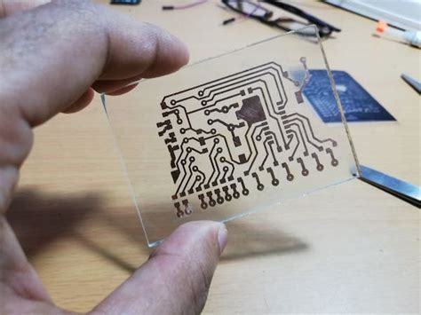
Allow the board to cool, then carefully peel off the transfer paper. The PCB design should now be transferred to the copper board. Touch up any imperfections with a permanent marker.
Step 3: Etch the PCB
-
Put on rubber gloves and safety glasses. Pour the ferric chloride solution into the plastic container. The solution should be deep enough to fully submerge the PCB.
-
Place the PCB into the solution with the copper side facing up. Agitate the container gently to ensure even etching.
-
The etching process usually takes 15-30 minutes depending on the solution strength and amount of copper to be removed. Monitor the etching progress and remove the PCB once all the unwanted copper has dissolved.
-
Rinse the etched PCB thoroughly with water. Dispose of the used etchant properly as it is toxic. Do not pour it down the drain.
-
Use fine grit sandpaper or a fiberglass scratch pad to remove the remaining toner, exposing the etched copper traces.
Step 4: Drill Holes and Apply Solder Mask (Optional)
-
Drill any necessary holes in the PCB for mounting components and vias using a drill or drill press. Use a drill bit slightly larger than the component leads.
-
If desired, apply a solder mask to protect the copper traces and prevent oxidation. Solder mask is available in paint or spray form and is applied over the etched PCB.

PCB Etching Tips and Troubleshooting
- If the transfer paper doesn’t peel off cleanly after ironing, try soaking the board in warm water to soften the paper.
- Adjust the strength of the ferric chloride solution if etching is too slow or too aggressive. A weak solution will take longer to etch while a strong solution may over-etch and damage fine traces.
- Regularly stir or agitate the etchant solution to prevent “dead spots” and ensure even etching.
- For complex or double-sided PCBs, consider using a professional PCB fabrication service instead of etching at home.
- Ventilate the work area well and wear gloves when handling chemicals. Ferric chloride can stain skin and surfaces.
Frequently Asked Questions (FAQ)
1. Can I reuse ferric chloride for etching multiple PCBs?
Yes, ferric chloride solution can be reused for etching several PCBs. However, the etching process will become slower as the solution weakens over time. Replenish or replace the solution as needed.
2. How do I dispose of used ferric chloride safely?
Ferric chloride is considered hazardous waste and should not be poured down the drain. Contact your local waste management facility for guidelines on proper disposal of ferric chloride in your area. Many communities have designated collection sites for household hazardous waste.
3. Can I use a regular paper instead of glossy or transfer paper?
No, regular paper will not work well for transferring the PCB design. The toner will not adhere properly to the copper board. Glossy paper or specially coated PCB transfer paper is required for best results.
4. How can I make double-sided PCBs at home?
To make double-sided PCBs, print and transfer the artwork for each side separately. After etching one side, drill alignment holes and use them to align the artwork for the second side. Then etch the second side. For connecting traces between sides, use through-hole rivets or manually solder wires through the holes.
5. What are some alternatives to ferric chloride for etching PCBs?
Other chemicals that can be used for etching copper PCBs include:
– Ammonium persulfate
– Hydrogen peroxide and hydrochloric acid (HCl) mixture
– Muriatic acid and hydrogen peroxide
– Copper chloride
– Sodium persulfate
However, some of these chemicals are more hazardous or difficult to obtain compared to ferric chloride. Proper safety precautions are crucial when using any etching chemicals.
Conclusion
PCB etching is a valuable skill for electronics enthusiasts and hobbyists looking to create custom circuit boards. With some basic tools, materials, and patience, it is possible to etch high-quality PCBs at home using the ferric chloride method outlined in this guide.
Remember to always prioritize safety and follow proper procedures when working with hazardous chemicals. With practice, you’ll be able to design and etch your own PCBs for projects, prototypes, and more.
For complex, multilayer, or large-scale PCB fabrication, it is still advisable to use professional PCB manufacturing services. But for simpler circuits and personal projects, etching your own PCBs can be a rewarding and cost-effective solution.


Leave a Reply