Introduction to Digital Image Correlation in PCB Manufacturing
Digital Image Correlation (DIC) is an optical technique used to measure deformation and strain on various materials and structures, including printed circuit boards (PCBs). In the PCB manufacturing industry, DIC has gained significant attention due to its non-contact, full-field, and high-accuracy measurement capabilities. With the increasing demand for Lead-Free PCBs, DIC has become an essential tool for evaluating and optimizing the manufacturing process, ensuring the production of high-quality and reliable PCBs.
What is Digital Image Correlation?
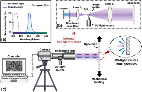
Digital Image Correlation is a non-contact optical technique that uses digital images to measure the deformation and strain of a material or structure. The process involves capturing a series of images of the object before and after deformation, and then analyzing the images using specialized software. The software tracks the movement of pixel patterns within the images and calculates the displacement and strain fields based on the changes in the pixel positions.
Advantages of Digital Image Correlation in PCB Manufacturing
-
Non-contact measurement: DIC allows for non-contact measurement of deformation and strain, eliminating the need for physical contact with the PCB, which could potentially damage the surface or alter the material properties.
-
Full-field measurement: DIC provides full-field measurement, allowing for the simultaneous measurement of deformation and strain across the entire surface of the PCB. This enables a comprehensive understanding of the material’s behavior under various loading conditions.
-
High accuracy: DIC offers high-accuracy measurements, with typical strain resolutions of 0.01% or better. This level of accuracy is essential for detecting and quantifying small deformations and strains in PCBs.
-
Versatility: DIC can be applied to a wide range of materials and structures, including PCBs of various sizes, shapes, and compositions. This versatility makes DIC a valuable tool for PCB manufacturers, allowing them to optimize their manufacturing processes for different types of PCBs.
Benefits of Digital Image Correlation in Lead-free PCB Manufacturing
1. Optimization of the Reflow Soldering Process
Lead-free soldering has become the standard in PCB manufacturing due to environmental and health concerns associated with lead-based solders. However, lead-free solders have higher melting temperatures and different mechanical properties compared to their lead-based counterparts, which can lead to challenges in the reflow soldering process. DIC can be used to optimize the reflow soldering process for lead-free PCBs by:
- Measuring the thermal expansion and contraction of the PCB during the reflow process
- Identifying areas of high stress and strain concentration
- Evaluating the effectiveness of different reflow profiles and parameters
- Optimizing the reflow process to minimize thermal stress and warpage
By using DIC to optimize the reflow soldering process, PCB manufacturers can improve the quality and reliability of their lead-free PCBs, reducing the occurrence of defects such as warpage, cracking, and delamination.
2. Evaluation of PCB Warpage and Flatness
Warpage and flatness are critical factors in PCB manufacturing, as they can affect the assembly process and the overall reliability of the final product. Lead-free PCBs are particularly susceptible to warpage due to the higher melting temperatures of lead-free solders and the differences in thermal expansion coefficients between the PCB substrate and components. DIC can be used to evaluate PCB warpage and flatness by:
- Measuring the out-of-plane deformation of the PCB during the manufacturing process
- Identifying areas of high warpage and determining the root causes
- Evaluating the effectiveness of different techniques for minimizing warpage, such as optimizing the layer stack-up or using warpage control materials
- Monitoring the flatness of the PCB during the assembly process to ensure proper component placement and soldering
By using DIC to evaluate PCB warpage and flatness, manufacturers can identify and address issues early in the manufacturing process, reducing the occurrence of defects and improving the overall quality of their lead-free PCBs.
3. Characterization of PCB Material Properties
The mechanical and thermal properties of PCB materials play a critical role in the performance and reliability of lead-free PCBs. DIC can be used to characterize the material properties of PCBs, providing valuable information for material selection and process optimization. Some of the material properties that can be characterized using DIC include:
- Elastic modulus
- Poisson’s ratio
- Coefficient of thermal expansion (CTE)
- Fracture toughness
- Fatigue properties
By using DIC to characterize PCB material properties, manufacturers can select the most suitable materials for their lead-free PCBs and optimize their manufacturing processes accordingly. This can lead to improved PCB performance, reliability, and durability.
4. Evaluation of PCB Mechanical Reliability
The mechanical reliability of PCBs is critical for ensuring the long-term performance and durability of electronic devices. Lead-free PCBs are subjected to various mechanical stresses during the manufacturing process and in-service conditions, which can lead to defects such as cracking, delamination, and pad cratering. DIC can be used to evaluate the mechanical reliability of PCBs by:
- Measuring the strain distribution in the PCB under various loading conditions, such as bending, twisting, and vibration
- Identifying areas of high stress concentration and potential failure sites
- Evaluating the effectiveness of different design and manufacturing techniques for improving mechanical reliability, such as using reinforced materials or optimizing the component layout
- Monitoring the PCB’s mechanical performance during accelerated life testing to assess its long-term reliability
By using DIC to evaluate the mechanical reliability of PCBs, manufacturers can identify and address potential issues early in the design and manufacturing process, leading to the production of more robust and reliable lead-free PCBs.
5. Quality Control and Failure Analysis
DIC can be used as a powerful tool for quality control and failure analysis in lead-free PCB manufacturing. By incorporating DIC into the quality control process, manufacturers can:
- Perform non-destructive testing of PCBs to identify defects and inconsistencies
- Measure the dimensional stability of PCBs during the manufacturing process to ensure compliance with specifications
- Evaluate the effectiveness of different quality control techniques and procedures
- Conduct failure analysis on defective or failed PCBs to determine the root causes and implement corrective actions
By using DIC for quality control and failure analysis, PCB manufacturers can improve the overall quality and reliability of their lead-free PCBs, reducing the occurrence of defects and failures, and ultimately leading to higher customer satisfaction and lower manufacturing costs.
Frequently Asked Questions (FAQ)
- Q: What are the main advantages of using Digital Image Correlation in PCB manufacturing?
A: The main advantages of using DIC in PCB manufacturing include non-contact measurement, full-field measurement, high accuracy, and versatility. These advantages allow for comprehensive evaluation and optimization of the manufacturing process, leading to improved PCB Quality and reliability.
- Q: How can Digital Image Correlation help optimize the reflow soldering process for lead-free PCBs?
A: DIC can be used to measure thermal expansion and contraction, identify areas of high stress and strain, evaluate the effectiveness of different reflow profiles, and optimize the reflow process to minimize thermal stress and warpage. By optimizing the reflow soldering process, manufacturers can reduce the occurrence of defects and improve the quality of their lead-free PCBs.
- Q: What PCB material properties can be characterized using Digital Image Correlation?
A: DIC can be used to characterize various PCB material properties, including elastic modulus, Poisson’s ratio, coefficient of thermal expansion (CTE), fracture toughness, and fatigue properties. By characterizing these properties, manufacturers can select the most suitable materials and optimize their manufacturing processes accordingly.
- Q: How can Digital Image Correlation be used for quality control and failure analysis in lead-free PCB manufacturing?
A: DIC can be used for non-destructive testing of PCBs, measuring dimensional stability, evaluating the effectiveness of quality control techniques, and conducting failure analysis on defective or failed PCBs. By incorporating DIC into the quality control process, manufacturers can improve the overall quality and reliability of their lead-free PCBs.
- Q: What are the potential benefits of using Digital Image Correlation in lead-free PCB manufacturing?
A: The potential benefits of using DIC in lead-free PCB manufacturing include improved PCB quality and reliability, reduced occurrence of defects and failures, higher customer satisfaction, and lower manufacturing costs. By leveraging the capabilities of DIC, manufacturers can optimize their manufacturing processes and produce high-quality lead-free PCBs.

Conclusion
Digital Image Correlation is a powerful tool that offers numerous benefits in lead-free PCB manufacturing. By utilizing DIC, manufacturers can optimize their reflow soldering process, evaluate PCB warpage and flatness, characterize material properties, assess mechanical reliability, and improve quality control and failure analysis. These benefits ultimately lead to the production of high-quality, reliable lead-free PCBs that meet the demanding requirements of modern electronic devices.
As the electronics industry continues to evolve and the demand for lead-free PCBs grows, the adoption of Digital Image Correlation in PCB manufacturing is expected to increase. By staying at the forefront of this technology and leveraging its capabilities, PCB manufacturers can gain a competitive edge, improve their manufacturing processes, and deliver superior products to their customers.
Leave a Reply