Introduction to PCB Prototyping
Printed Circuit Board (PCB) prototyping is a crucial step in the development of new electronic products. It allows designers and engineers to test and refine their designs before committing to full-scale production. PCB prototyping involves creating a small batch of boards that can be used for testing, debugging, and validation of the design. In this article, we will delve into the details of PCB prototyping and how it can help you build a new product quickly and efficiently.
The Importance of PCB Prototyping
PCB prototyping is an essential part of the product development process for several reasons:
-
Design Validation: Prototyping allows you to validate your design and ensure that it works as intended. You can test the functionality, performance, and reliability of your design before moving to mass production.
-
Cost Savings: By identifying and fixing issues early in the development process, you can avoid costly mistakes and rework during mass production. Prototyping helps you optimize your design, reducing the overall cost of production.
-
Time-to-Market: PCB prototyping enables you to quickly iterate on your design and bring your product to market faster. By parallelizing the prototyping and testing phases, you can shorten the overall development time.
-
Risk Mitigation: Prototyping helps mitigate risks associated with new product development. You can identify potential problems and address them before they become significant issues in production.
The PCB Prototyping Process
The PCB prototyping process typically involves the following steps:
1. Design Creation
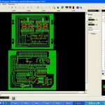
The first step in PCB prototyping is to create a design using Electronic Design Automation (EDA) software. This involves schematic capture, component selection, and PCB layout. The design should be optimized for manufacturing and tested for functionality and performance.
2. Design Review
Once the design is complete, it undergoes a thorough review process. This includes checking for design rule violations, manufacturability, and compatibility with the intended application. Any issues identified during the review process are addressed before moving to the next step.
3. Prototype Fabrication
After the design review, the PCB Prototype is fabricated. This involves the following sub-steps:
-
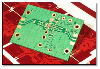
PCB Fabrication: The PCB is manufactured using a specialized process that involves printing the circuit pattern on a copper-clad board, etching away the unwanted copper, and drilling holes for components.
-
PCB Assembly: The components are placed and soldered onto the PCB using either through-hole or surface-mount technology (SMT).
-
Inspection and Testing: The assembled PCB is inspected for quality and tested for functionality and performance.
4. Prototype Validation
Once the prototype is fabricated, it undergoes a series of validation tests to ensure that it meets the design specifications. This includes functional testing, environmental testing, and reliability testing. Any issues identified during validation are addressed before moving to the next step.
5. Design Refinement
Based on the results of the validation tests, the design may need to be refined. This may involve minor tweaks to the component selection, PCB layout, or firmware. The refined design then goes through another round of prototyping and validation.
6. Production-Ready Design
Once the design has been refined and validated, it is ready for mass production. The final design package includes the schematic, PCB layout, bill of materials (BOM), and assembly instructions.

Choosing a PCB Prototyping Partner
Choosing the right PCB prototyping partner is crucial to the success of your project. Here are some factors to consider when selecting a partner:
-
Experience: Look for a partner with experience in PCB prototyping and a track record of successful projects.
-
Capabilities: Ensure that the partner has the capabilities and equipment needed to fabricate and assemble your PCB prototype.
-
Quality: Choose a partner that adheres to strict quality standards and has a robust quality control process.
-
Communication: Look for a partner that communicates clearly and regularly throughout the prototyping process.
-
Turnaround Time: Consider the partner’s turnaround time and ensure that it aligns with your project timeline.
PCB Prototyping Techniques
There are several PCB prototyping techniques that can be used depending on the complexity of the design and the required turnaround time:
1. Quick-Turn PCB Prototyping
Quick-turn PCB prototyping is a fast and cost-effective way to get a small batch of PCBs fabricated and assembled. This technique is suitable for simple designs that do not require extensive testing or validation. Quick-turn prototyping can typically be completed in 1-5 days.
2. Multi-Layer PCB Prototyping
Multi-layer PCB prototyping is used for more complex designs that require multiple layers of circuitry. This technique involves bonding several layers of PCBs together to create a single, high-density board. Multi-layer prototyping is more expensive and time-consuming than quick-turn prototyping but offers better performance and reliability.
3. Flexible PCB Prototyping
Flexible PCB prototyping is used for designs that require flexibility or conformity to a specific shape. This technique involves using a flexible substrate material instead of a rigid PCB. Flexible PCBs are more challenging to fabricate and assemble than rigid PCBs but offer unique advantages in certain applications.
PCB Prototyping vs. PCB Manufacturing
While PCB prototyping and PCB manufacturing are related, they serve different purposes in the product development process. Here are some key differences between the two:
| PCB Prototyping | PCB Manufacturing |
|---|---|
| Small batch production | Large-scale production |
| Used for testing and validation | Used for final product |
| Quick turnaround time | Longer lead times |
| Higher cost per unit | Lower cost per unit |
| Lower tooling costs | Higher tooling costs |
| More forgiving of design changes | Less forgiving of design changes |
Benefits of PCB Prototyping
PCB prototyping offers several benefits to product developers:
-
Faster Time-to-Market: By enabling quick design iterations and validation, PCB prototyping helps bring products to market faster.
-
Reduced Development Costs: Prototyping allows for early identification and correction of design issues, reducing the overall cost of development.
-
Improved Product Quality: Prototyping enables thorough testing and validation of the design, resulting in a higher-quality final product.
-
Increased Confidence: Prototyping provides tangible evidence of the design’s functionality and performance, increasing confidence in the final product.
Common Pitfalls in PCB Prototyping
While PCB prototyping offers many benefits, there are also some common pitfalls to avoid:
-
Inadequate Design Review: Failing to thoroughly review the design before prototyping can lead to costly rework and delays.
-
Poor Component Selection: Choosing the wrong components or using obsolete parts can result in performance issues and supply chain problems.
-
Incorrect PCB Layout: Laying out the PCB incorrectly can lead to signal integrity issues, electromagnetic interference (EMI), and thermal problems.
-
Insufficient Testing: Failing to adequately test the prototype can result in undetected issues that manifest in the final product.
-
Rushing the Process: Attempting to rush the prototyping process can lead to mistakes and oversights that compromise the quality of the final product.
FAQ
Q1. How long does PCB prototyping take?
A1. The turnaround time for PCB prototyping depends on the complexity of the design and the chosen prototyping technique. Quick-turn prototyping can typically be completed in 1-5 days, while more complex designs may take several weeks.
Q2. How much does PCB prototyping cost?
A2. The cost of PCB prototyping varies depending on the size and complexity of the design, the chosen prototyping technique, and the number of prototypes required. Quick-turn prototyping is generally less expensive than multi-layer or flexible PCB prototyping.
Q3. Can I use PCB prototyping for small-scale production?
A3. Yes, PCB prototyping can be used for small-scale production runs of up to a few hundred units. However, for larger production runs, it is generally more cost-effective to use traditional PCB manufacturing techniques.
Q4. What files do I need to provide for PCB prototyping?
A4. To begin the PCB prototyping process, you will typically need to provide the following files: schematic, PCB layout (Gerber files), bill of materials (BOM), and assembly instructions.
Q5. Can I make changes to my design during the prototyping process?
A5. Yes, one of the benefits of PCB prototyping is that it allows for design changes and refinements based on the results of testing and validation. However, making changes during the prototyping process may increase the turnaround time and cost.
Conclusion
PCB prototyping is a vital step in the development of new electronic products. It enables designers and engineers to test and refine their designs before committing to full-scale production, reducing the risk of costly mistakes and delays. By following the PCB prototyping process and choosing the right prototyping partner and technique, you can quickly and efficiently bring your new product to market.
Leave a Reply