What is a PCB Prototype?
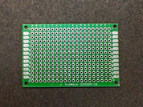
A PCB (Printed Circuit Board) prototype is a preliminary version of a printed circuit board designed to test and validate the functionality, performance, and manufacturability of the final product. It is an essential step in the development process of electronic devices, allowing engineers to identify and resolve any issues before mass production begins.
PCB prototypes are typically smaller in scale compared to the final production version and may not include all the features or components of the finished product. However, they provide a crucial opportunity to assess the board’s layout, component placement, signal integrity, and overall functionality.
Benefits of PCB Prototyping
-
Design Validation: PCB prototypes allow engineers to test and validate their design before committing to full-scale production. This helps identify any design flaws, component incompatibilities, or performance issues early in the development process.
-
Cost Savings: By identifying and resolving issues during the prototyping phase, companies can avoid costly mistakes and rework in mass production. Prototyping helps optimize the design, reducing the risk of manufacturing defects and minimizing waste.
-
Functionality Testing: Prototypes enable engineers to test the board’s functionality under real-world conditions. This includes verifying signal integrity, power distribution, and thermal management, ensuring the final product meets the desired specifications.
-
Manufacturability Assessment: PCB prototyping allows manufacturers to assess the feasibility of the design for mass production. They can identify any potential challenges in the assembly process, such as component placement or soldering requirements, and make necessary adjustments.
-
Accelerated Time-to-Market: By iterating and refining the design through prototyping, companies can accelerate the development process and bring their products to market faster. Prototyping helps streamline the transition from concept to final production.
Industrial PCB Prototype Applications
Industrial PCB prototypes find applications across various sectors, including:
-
Automotive Electronics: Prototyping is crucial for developing reliable and robust electronic systems for vehicles, such as engine control units, infotainment systems, and advanced driver assistance systems (ADAS).
-
Industrial Automation: PCB prototypes are used to develop and test control systems, sensors, and communication modules for industrial automation equipment, ensuring reliable operation in harsh environments.
-
Medical Devices: Prototyping is essential for developing medical devices that meet stringent safety and performance requirements. PCB prototypes help validate the functionality and reliability of devices such as patient monitors, diagnostic equipment, and wearable sensors.
-
Aerospace and Defense: PCB prototypes are used to develop and test avionics systems, radar modules, and communication equipment for aerospace and defense applications, ensuring they meet the demanding requirements of these industries.
-
Internet of Things (IoT): Prototyping is crucial for developing IoT devices, such as smart sensors, connected appliances, and wearable technology. PCB prototypes help validate the functionality, connectivity, and power efficiency of these devices.
PCB Prototype Manufacturing Process
The PCB prototype manufacturing process typically involves the following steps:
-
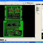
Design and Layout: Engineers create the schematic design and PCB layout using electronic design automation (EDA) software. The layout defines the placement of components, traces, and vias on the board.
-
Fabrication: The PCB prototype is fabricated using a combination of processes, including:
- Etching: The copper-clad laminate is selectively etched to create the conductive traces and pads based on the PCB layout.
- Drilling: Holes are drilled through the board to accommodate through-hole components and vias.
- Plating: The drilled holes are plated with a conductive material, typically copper, to establish electrical connections between layers.
- Solder Mask Application: A protective solder mask layer is applied to the board to prevent short circuits and improve solderability.
-
Silkscreen Printing: Text, symbols, and component designators are printed on the board using silkscreen printing for easy identification during assembly.
-
Assembly: The PCB prototype is populated with components, either through manual soldering or automated assembly processes such as surface mount technology (SMT) or through-hole technology (THT).
-
Testing and Inspection: The assembled prototype undergoes rigorous testing and inspection to verify its functionality, performance, and quality. This may include visual inspection, automated optical inspection (AOI), and functional testing using specialized equipment.
-
Rework and Refinement: Based on the testing results, engineers may need to rework or refine the design to address any issues or improve performance. This may involve modifying the component placement, adjusting trace widths, or optimizing the power distribution network.
-
Final Validation: Once the PCB prototype meets the desired specifications and passes all tests, it is considered validated and ready for transition to mass production.

PCB Prototype Manufacturing Techniques
There are several manufacturing techniques used for PCB prototyping, each with its own advantages and considerations:
1. Quick-Turn PCB Prototyping
Quick-turn PCB prototyping, also known as rapid prototyping, focuses on delivering PCB prototypes in a short timeframe, typically within a few days. This technique is ideal for projects with tight deadlines or when multiple iterations are required.
Key characteristics of quick-turn PCB prototyping include:
– Streamlined manufacturing processes to minimize turnaround time
– Use of automated design rule checks (DRC) to identify and resolve design issues quickly
– Prioritization of speed over cost optimization
2. High-Density Interconnect (HDI) PCB Prototyping
HDI PCB prototyping involves the fabrication of PCBs with high-density interconnects, enabling the integration of more components and functionality in a smaller form factor. HDI PCBs use advanced manufacturing techniques, such as microvias and fine-pitch traces, to achieve high component density.
Key characteristics of HDI PCB prototyping include:
– Ability to accommodate a large number of components in a compact size
– Improved signal integrity and reduced signal interference
– Suitable for applications requiring miniaturization and high performance
3. Flexible PCB Prototyping
Flexible PCB prototyping involves the fabrication of PCBs that can bend, flex, and conform to various shapes. Flexible PCBs are made using flexible substrate materials, such as polyimide or polyester, and are ideal for applications requiring flexibility or space constraints.
Key characteristics of flexible PCB prototyping include:
– Ability to bend and conform to desired shapes
– Lightweight and thin form factor
– Suitable for wearable devices, medical implants, and aerospace applications
4. Rigid-Flex PCB Prototyping
Rigid-flex PCB prototyping combines the benefits of both rigid and flexible PCBs. These PCBs consist of rigid sections connected by flexible interconnects, allowing for three-dimensional configurations and improved reliability.
Key characteristics of rigid-flex PCB prototyping include:
– Combination of rigid and flexible sections in a single board
– Ability to fold and conform to specific shapes
– Enhanced durability and resistance to vibration and shock
PCB Prototype Testing and Validation
Testing and validation are critical steps in the PCB prototyping process to ensure the functionality, performance, and reliability of the final product. Some common testing techniques include:
1. Visual Inspection
Visual inspection involves examining the PCB prototype for any visible defects, such as incomplete etching, short circuits, or damaged components. This can be done manually or using automated optical inspection (AOI) systems.
2. Continuity Testing
Continuity testing verifies the electrical connections between components and ensures there are no open circuits or short circuits. This is typically done using a multimeter or a dedicated continuity tester.
3. Functional Testing
Functional testing involves powering up the PCB prototype and verifying that it performs as intended. This may include testing specific features, inputs, outputs, and communication interfaces.
4. Signal Integrity Testing
Signal integrity testing assesses the quality of the electrical signals transmitted through the PCB. It involves measuring parameters such as signal rise time, fall time, and propagation delay to ensure the signals remain within acceptable limits.
5. Environmental Testing
Environmental testing exposes the PCB prototype to various environmental conditions, such as temperature extremes, humidity, and vibration, to assess its durability and reliability. This helps identify any potential weaknesses or failure points.
PCB Prototype Design Considerations
When designing a PCB prototype, engineers must consider several key factors to ensure optimal performance and manufacturability:
-
Component Selection: Choose components that meet the functional, performance, and reliability requirements of the application. Consider factors such as power dissipation, package size, and availability.
-
Layout and Routing: Optimize the placement of components and routing of traces to minimize signal interference, ensure proper power distribution, and facilitate efficient manufacturing. Follow best practices for trace width, spacing, and via placement.
-
Signal Integrity: Ensure the integrity of the electrical signals by minimizing crosstalk, reflections, and noise. Use appropriate impedance matching techniques and consider the use of ground planes and shielding.
-
Thermal Management: Consider the thermal requirements of the components and design the PCB to facilitate proper heat dissipation. This may involve the use of thermal vias, heatsinks, or other cooling techniques.
-
Manufacturing Constraints: Design the PCB prototype with manufacturing constraints in mind, such as minimum trace width, hole size, and component spacing. Consult with the PCB manufacturer to ensure the design is compatible with their fabrication capabilities.
-
Testing and Debugging: Incorporate test points and debugging features into the PCB prototype design to facilitate testing and troubleshooting. This may include the use of test pads, JTAG interfaces, or diagnostic LEDs.
Frequently Asked Questions (FAQ)
-
What is the typical turnaround time for PCB prototype manufacturing?
The turnaround time for PCB prototype manufacturing varies depending on the complexity of the design and the manufacturing technique used. Quick-turn prototyping services can deliver prototypes within a few days, while more complex designs may take several weeks. -
How much does it cost to manufacture a PCB prototype?
The cost of manufacturing a PCB prototype depends on factors such as the board size, layer count, component density, and manufacturing technique. Quick-turn prototyping services may have higher costs due to expedited manufacturing, while larger quantities or simpler designs may have lower per-unit costs. -
What files are required for PCB prototype manufacturing?
To manufacture a PCB prototype, the following files are typically required: - Gerber files: These files contain the PCB layout information, including copper layers, solder mask, and silkscreen.
- Drill files: These files specify the location, size, and type of holes to be drilled in the PCB.
- Bill of Materials (BOM): The BOM lists all the components required for the PCB Assembly, including their quantities, part numbers, and specifications.
-
Assembly drawings: These drawings provide instructions for component placement and orientation during the assembly process.
-
Can PCB prototypes be used for final production?
PCB prototypes are primarily used for testing, validation, and design refinement purposes. While they may functionally resemble the final product, they may not be optimized for mass production. Final production may require additional optimization, such as design for manufacturing (DFM) considerations and cost reduction efforts. -
How can I ensure the reliability of my PCB prototype?
To ensure the reliability of your PCB prototype, consider the following: - Conduct thorough testing and validation, including functional testing, environmental testing, and signal integrity analysis.
- Use high-quality components from reputable suppliers to minimize the risk of failures.
- Follow best practices for PCB design, including proper component placement, trace routing, and thermal management.
- Work with experienced PCB manufacturing partners who adhere to strict quality control standards and have a proven track record of delivering reliable prototypes.
| PCB Prototype Manufacturing Technique | Advantages | Considerations |
|---|---|---|
| Quick-Turn PCB Prototyping | Fast turnaround time Ideal for multiple iterations |
Higher costs Limited complexity |
| High-Density Interconnect (HDI) PCB Prototyping | High component density Improved signal integrity |
Higher manufacturing costs Requires advanced manufacturing capabilities |
| Flexible PCB Prototyping | Flexibility and conformability Lightweight and thin form factor |
Limited component placement options Requires specialized assembly techniques |
| Rigid-Flex PCB Prototyping | Combination of rigid and flexible sections Enhanced durability |
Higher manufacturing costs Complex design and assembly process |
In conclusion, industrial PCB prototyping is a critical step in the development of electronic devices, enabling engineers to test, validate, and refine their designs before proceeding to mass production. By leveraging various manufacturing techniques, such as quick-turn prototyping, HDI PCB prototyping, flexible PCB prototyping, and rigid-flex PCB prototyping, companies can create prototypes that meet their specific requirements and accelerate the development process. Through rigorous testing, validation, and design optimization, PCB prototypes help ensure the functionality, performance, and reliability of the final product, ultimately leading to successful market adoption and customer satisfaction.
Leave a Reply