Introduction to PCB Component Placement
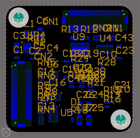
Printed circuit board (PCB) layout is a critical step in the design and manufacturing of electronic devices. Proper component placement on the PCB is essential for ensuring optimal electrical performance, signal integrity, manufacturability, and reliability of the final product.
In this comprehensive guide, we will dive into the key principles and best practices for PCB component placement. Whether you are a novice designer or an experienced engineer, understanding these guidelines will help you create robust and efficient PCB layouts that meet your design requirements.
Factors to Consider When Placing Components on a PCB
When placing components on a PCB, several factors must be taken into account to ensure a successful design. These factors include:
Electrical Performance
The primary goal of PCB component placement is to achieve the desired electrical performance of the circuit. This involves considering signal integrity, power distribution, EMI/EMC, and thermal management.
Manufacturing Constraints
PCB manufacturing processes impose certain limitations on component placement. For example, components must be spaced apart sufficiently to allow for automated assembly machines to pick and place them accurately. Additionally, Component Orientation and placement should facilitate easy soldering and inspection.
Mechanical Constraints
The mechanical design of the enclosure or housing for the PCB may dictate specific component locations and orientations. Connectors, switches, and indicators are often placed along the edges of the board for easy access. The placement of tall components, such as capacitors or heat sinks, must also consider clearance requirements.
Cost Considerations
Component placement can impact the overall cost of the PCB. Minimizing the board size, reducing the number of layers, and optimizing component placement for automated assembly can help lower manufacturing costs.
Best Practices for PCB Component Placement
Now that we have covered the key factors to consider, let’s explore some best practices for placing components on a PCB.
Group Related Components Together
Components that are functionally related or belong to the same sub-circuit should be placed close together. This minimizes the length of traces connecting them, reduces parasitic effects, and improves signal integrity. For example, place decoupling capacitors near their corresponding ICs, and keep analog and digital sections separate.
Minimize Trace Lengths
Shorter traces between components lead to better signal integrity, reduced electromagnetic interference (EMI), and improved overall performance. When placing components, aim to minimize the distance between connected pins. This is particularly important for high-speed signals and sensitive analog circuits.
Consider Signal Flow
Place components in a logical sequence that follows the signal flow of the circuit. This helps in understanding the circuit’s functionality and makes debugging and troubleshooting easier. Start with the input components, such as connectors or sensors, and progress towards the output components, like indicators or actuators.
Optimize for Manufacturing
To ensure smooth and reliable manufacturing, follow these guidelines:
- Provide sufficient spacing between components for automated assembly machines.
- Orient components in the same direction whenever possible to simplify the assembly process.
- Place SMD components on the same side of the board to minimize the number of assembly steps.
- Keep component placement consistent across similar designs to reduce setup time and errors.
Thermal Management
Heat-generating components, such as power regulators, transistors, and high-speed processors, should be placed strategically to dissipate heat effectively. Consider the following:
- Place heat-generating components near the edges of the board for better airflow.
- Use thermal vias or heat sinks to conduct heat away from critical components.
- Provide adequate spacing around heat-generating components to avoid thermal coupling with nearby components.
Electromagnetic Compatibility (EMC)
Proper component placement can help mitigate EMI and ensure EMC compliance. Follow these tips:
- Separate noisy components, like switching regulators, from sensitive analog circuits.
- Use ground planes and shielding techniques to reduce electromagnetic interference.
- Place decoupling capacitors close to ICs to suppress high-frequency noise.
Connector Placement
Connectors should be placed along the edges of the board for easy access and cable management. Consider the following:
- Ensure sufficient clearance around connectors for mating and unmating.
- Orient connectors to minimize strain on the PCB and cables.
- Group related connectors together for intuitive user interaction.

PCB Component Placement Checklist
To ensure you have covered all the essential aspects of PCB component placement, refer to this handy checklist:
- [ ] Group related components together
- [ ] Minimize trace lengths
- [ ] Follow logical signal flow
- [ ] Optimize for manufacturing
- [ ] Address thermal management
- [ ] Consider EMC requirements
- [ ] Place connectors strategically
- [ ] Review mechanical constraints
- [ ] Verify electrical performance
- [ ] Optimize for cost
PCB Component Placement Tools and Software
Several PCB design software packages offer powerful tools to assist with component placement. Some popular options include:
| Software | Vendor | Key Features |
|---|---|---|
| Altium Designer | Altium | Advanced 3D placement, rule-driven design, real-time DRC |
| EAGLE | Autodesk | Schematic-driven layout, extensive component libraries |
| KiCad | Open Source | Free and open-source, integrated schematic and layout editors |
| OrCAD PCB Designer | Cadence | Constraint-driven layout, advanced routing capabilities |
These tools provide features like automatic component placement, design rule checking (DRC), 3D visualization, and integration with schematic capture and simulation software.
Frequently Asked Questions (FAQ)
1. What is the importance of PCB component placement?
Proper PCB component placement is crucial for several reasons:
- Ensuring optimal electrical performance and signal integrity
- Facilitating efficient manufacturing and assembly processes
- Minimizing electromagnetic interference (EMI) and ensuring EMC compliance
- Enabling effective thermal management and Heat Dissipation
- Achieving a compact and cost-effective board design
2. How does component placement affect signal integrity?
Component placement directly impacts signal integrity in the following ways:
- Shorter traces between components minimize parasitic effects and signal distortion.
- Proper placement of decoupling capacitors near ICs suppresses high-frequency noise.
- Separating analog and digital sections reduces crosstalk and interference.
- Strategic placement of termination resistors and impedance-controlled traces maintains signal quality.
3. What are some common mistakes to avoid in PCB component placement?
Some common mistakes to avoid when placing components on a PCB include:
- Placing components too close together, making assembly and soldering difficult.
- Neglecting thermal management and placing heat-generating components too close to sensitive devices.
- Failing to consider the mechanical constraints of the enclosure or housing.
- Overlooking the impact of component placement on EMI and EMC.
- Not optimizing component placement for automated assembly, leading to higher manufacturing costs.
4. How can I optimize my PCB layout for automated assembly?
To optimize your PCB layout for automated assembly, follow these guidelines:
- Provide sufficient spacing between components to allow for Pick-and-Place machines.
- Orient components in the same direction whenever possible.
- Place SMD components on the same side of the board to minimize the number of assembly steps.
- Use standardized component packages and footprints.
- Keep component placement consistent across similar designs to reduce setup time.
5. What are some best practices for placing connectors on a PCB?
When placing connectors on a PCB, consider the following best practices:
- Place connectors along the edges of the board for easy access and cable management.
- Ensure adequate clearance around connectors for mating and unmating.
- Orient connectors to minimize strain on the PCB and cables.
- Group related connectors together for intuitive user interaction.
- Consider the mechanical constraints of the enclosure and the location of cable entry points.
Conclusion
PCB component placement is a critical aspect of PCB design that directly impacts the performance, manufacturability, and reliability of electronic devices. By understanding the key factors to consider and following best practices, designers can create optimized PCB layouts that meet their design requirements while minimizing cost and time to market.
Remember to group related components together, minimize trace lengths, follow logical signal flow, optimize for manufacturing, address thermal management, consider EMC requirements, and place connectors strategically. Utilize PCB design software tools to assist with component placement and verify your design against industry standards and guidelines.
By mastering the art of PCB component placement, you can unlock the full potential of your Electronic Designs and create products that are efficient, reliable, and cost-effective.
Leave a Reply