Introduction to PCB Component Placement
Printed Circuit Board (PCB) component placement is a crucial step in the PCB Assembly process. It involves the precise positioning and orientation of electronic components on the PCB substrate. The primary goal of component placement is to ensure optimal electrical performance, mechanical stability, and manufacturability of the PCB assembly.
Importance of Proper Component Placement
Proper component placement is essential for several reasons:
- Electrical Performance: Optimal placement of components minimizes signal interference, crosstalk, and noise, leading to better electrical performance of the PCB.
- Mechanical Stability: Correctly placed components are less likely to suffer from mechanical stress, vibration, or thermal issues, enhancing the overall reliability of the PCB assembly.
- Manufacturability: Efficient component placement facilitates automated assembly processes, reduces manufacturing time and costs, and minimizes the risk of assembly errors.
PCB Component Placement Considerations
When placing components on a PCB, several factors must be taken into account to ensure optimal results. These considerations include:
1. Component Footprint and Orientation
Each component has a specific footprint that defines its physical dimensions and the arrangement of its leads or pads. It is crucial to ensure that the footprint of each component matches the corresponding pad pattern on the PCB layout. Additionally, the orientation of the component (e.g., pin 1 location) must be correctly aligned with the PCB layout to avoid assembly errors.
2. Placement Density and Spacing
The placement density refers to the number of components per unit area on the PCB. Higher placement densities can be achieved by using smaller components and tighter spacing between them. However, it is essential to maintain adequate spacing between components to ensure proper solderability, avoid short circuits, and facilitate heat dissipation.
| Component Package | Typical Spacing |
|---|---|
| Dual Inline Package (DIP) | 0.1 inch (2.54 mm) |
| Small Outline Integrated Circuit (SOIC) | 0.05 inch (1.27 mm) |
| Quad Flat Package (QFP) | 0.031 inch (0.8 mm) |
| Ball Grid Array (BGA) | 0.02 inch (0.5 mm) |
3. Thermal Management
Electronic components generate heat during operation, and proper thermal management is crucial for maintaining the reliability and performance of the PCB assembly. When placing components, consider their power dissipation and thermal characteristics. High-power components should be placed in areas with good airflow and away from temperature-sensitive components. If necessary, use thermal management techniques such as heat sinks, thermal vias, or copper pours to dissipate heat effectively.
4. Signal Integrity and EMI/EMC
Signal integrity refers to the quality of electrical signals transmitted through the PCB. To maintain signal integrity, critical components such as high-speed devices, clock sources, and sensitive analog circuits should be placed close to their respective connectors or ports. Proper grounding and shielding techniques should be employed to minimize electromagnetic interference (EMI) and ensure electromagnetic compatibility (EMC).
5. Manufacturing Constraints
PCB component placement must also consider manufacturing constraints such as assembly equipment capabilities, soldering techniques, and testability. For example, components should be placed in a manner that allows for automated Pick-and-Place machines to accurately position them during assembly. Adequate clearance should be provided for soldering tools, and test points should be accessible for automated testing and debugging.

PCB Component Placement Techniques
Several techniques can be employed to optimize component placement on a PCB. These include:
1. Grouping and Zoning
Components with similar functions or related circuitry should be grouped together to minimize the lengths of interconnects and improve signal integrity. Different functional blocks or subsystems can be separated into distinct zones on the PCB, making the layout more organized and easier to troubleshoot.
2. Placement for Manufacturing
To facilitate automated assembly processes, components should be placed in a manner that allows for efficient pick-and-place operations. This includes:
- Aligning components in a consistent direction to minimize the number of rotations required during placement.
- Placing components on the same side of the PCB whenever possible to reduce the number of assembly steps.
- Providing sufficient clearance around components for soldering and inspection.
3. Panelization and Depanelization
Panelization is the process of arranging multiple PCBs on a single panel for manufacturing efficiency. When placing components near the edges of individual PCBs, ensure that there is enough space for the depanelization process, which involves cutting the panel into individual boards. Avoid placing components too close to the board edges or in areas where mechanical stress may occur during depanelization.
4. Design for Test (DFT)
Design for Test (DFT) principles should be incorporated into the component placement process to enable efficient testing and debugging of the PCB assembly. This includes:
- Placing test points and probe pads in accessible locations.
- Providing clear markings or labels for components and test points.
- Ensuring that components do not obstruct access to test points or other critical areas of the PCB.

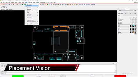
PCB Component Placement Tools and Software
Various tools and software solutions are available to assist in the PCB component placement process. These include:
1. Electronic Design Automation (EDA) Tools
EDA tools, such as Altium Designer, Cadence Allegro, or Mentor Graphics PADS, provide comprehensive PCB design and layout capabilities. These tools offer features like automatic component placement, design rule checking (DRC), and 3D visualization to optimize component placement and ensure adherence to design guidelines.
2. Placement Optimization Software
Specialized placement optimization software, such as Siemens Tecnomatix or Valor MSS, can analyze the PCB layout and suggest optimal component placements based on predefined rules and constraints. These tools consider factors like component size, shape, and thermal characteristics to generate efficient placement solutions.
3. Manufacturing Execution Systems (MES)
Manufacturing Execution Systems (MES) are software platforms that manage and optimize the PCB assembly process. MES solutions often include modules for component placement planning, machine programming, and real-time production monitoring. These tools help ensure that the component placement process is accurate, efficient, and aligned with manufacturing constraints.

Best Practices for PCB Component Placement
To achieve optimal results in PCB component placement, consider the following best practices:
- Start with a Well-Defined Schematic: Ensure that the schematic design is complete, accurate, and properly labeled before starting the component placement process.
- Consider the PCB Stack-up: Take into account the number of layers, layer thicknesses, and material properties of the PCB stack-up when placing components.
- Use a Consistent Grid System: Establish a consistent grid system for component placement to ensure proper alignment and spacing.
- Place Critical Components First: Begin by placing critical components such as connectors, power regulators, and high-speed devices, and then position other components around them.
- Route Power and Ground Early: Plan the power and ground routing early in the placement process to ensure proper power distribution and minimize noise.
- Minimize Crosstalk and Interference: Place components and route traces in a way that minimizes crosstalk and interference between signals.
- Consider Assembly and Manufacturing Constraints: Ensure that component placement is compatible with the capabilities of the assembly equipment and processes.
- Perform Design Rule Checks (DRC): Regularly perform DRC to identify and resolve any placement violations or conflicts.
- Collaborate with Stakeholders: Engage with other stakeholders, such as electrical engineers, mechanical designers, and manufacturing experts, to ensure that the component placement meets all requirements.
- Document and Communicate: Clearly document the component placement guidelines and communicate them to all relevant team members to ensure consistency and adherence to standards.
Frequently Asked Questions (FAQ)
-
What is the most important factor to consider when placing components on a PCB?
The most important factor to consider when placing components on a PCB is the electrical performance of the circuit. Proper component placement should minimize signal interference, crosstalk, and noise while ensuring optimal power distribution and grounding. -
How does component placement affect the manufacturability of a PCB?
Component placement directly impacts the manufacturability of a PCB. Proper placement should facilitate automated assembly processes, reduce the risk of assembly errors, and minimize manufacturing time and costs. Factors such as Component Orientation, spacing, and accessibility for soldering and testing should be considered to ensure efficient manufacturability. -
What are some common pitfalls to avoid in PCB component placement?
Some common pitfalls to avoid in PCB component placement include: - Placing components too close to each other, leading to solderability issues and short circuits.
- Neglecting thermal management, resulting in overheating and reduced reliability.
- Ignoring signal integrity and EMI/EMC considerations, causing signal degradation and interference.
-
Placing components in a way that hinders automated assembly or testing processes.
-
How can PCB design software help in optimizing component placement?
PCB design software, such as EDA tools, offers features like automatic component placement, design rule checking (DRC), and 3D visualization. These tools can analyze the PCB layout, suggest optimal component placements based on predefined rules and constraints, and help ensure adherence to design guidelines. They consider factors like component size, shape, and thermal characteristics to generate efficient placement solutions. -
What are some best practices for collaborating with other stakeholders during the component placement process?
To effectively collaborate with other stakeholders during the component placement process: - Involve all relevant stakeholders, such as electrical engineers, mechanical designers, and manufacturing experts, early in the design process.
- Clearly communicate the design requirements, constraints, and objectives to ensure everyone is aligned.
- Regularly review and discuss the component placement with stakeholders to gather feedback and address any concerns.
- Document the component placement guidelines and decisions to maintain consistency and facilitate knowledge sharing.
- Establish a version control system to track changes and revisions throughout the placement process.
Conclusion
PCB component placement is a critical step in the PCB assembly process, directly impacting the electrical performance, mechanical stability, and manufacturability of the final product. By considering factors such as component footprint, placement density, thermal management, signal integrity, and manufacturing constraints, designers can optimize the placement of components on the PCB.
Various techniques, such as grouping and zoning, placement for manufacturing, panelization, and design for test, can be employed to achieve optimal results. PCB design tools and software solutions assist in automating and optimizing the placement process, while collaboration with stakeholders ensures that all requirements are met.
By following best practices and leveraging the available tools and techniques, PCB designers can create efficient, reliable, and manufacturable PCB assemblies that meet the desired performance and quality standards.


Leave a Reply