Introduction to Telecom PCB Assembly (TPA)
Telecom PCB Assembly (TPA) is a crucial process in the manufacturing of printed circuit boards (PCBs) for the telecommunications industry. These PCBs are designed to meet the specific requirements of telecom equipment, such as high-speed data transmission, low signal loss, and reliable performance in harsh environments. TPA involves the assembly of various electronic components onto the PCB substrate, ensuring proper functionality and adherence to industry standards.
The Importance of TPA in the Telecom Industry
The telecommunications industry relies heavily on the proper functioning of PCBs in various devices, including:
- Mobile phones
- Routers
- Switches
- Base stations
- Satellite communication systems
TPA plays a vital role in ensuring that these devices operate efficiently and reliably, enabling seamless communication across networks.
The TPA Process
PCB Design and Layout
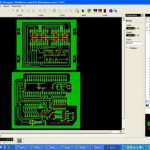
The first step in the TPA process is the design and layout of the PCB. This involves creating a schematic diagram that outlines the electrical connections between components and then translating this into a physical layout. The layout must consider factors such as signal integrity, power distribution, and thermal management.
Component Selection and Sourcing
Once the PCB design is finalized, the next step is to select and source the required electronic components. These components must meet the specific requirements of the telecom application, such as high-frequency operation, low noise, and high reliability. Components are typically sourced from approved vendors to ensure quality and consistency.
PCB Fabrication
The PCB substrate is fabricated using a combination of chemical and mechanical processes. This involves:
- Creating the copper traces on the substrate using photolithography
- Drilling holes for component placement
- Applying solder mask and silkscreen layers
The fabricated PCB is then inspected for defects and conformance to specifications.
Component Placement and Soldering
The sourced components are then placed onto the PCB substrate using automated pick-and-place machines. These machines use computer vision and precision robotics to accurately place components at high speeds. Once placed, the components are soldered to the PCB using either wave soldering or reflow soldering techniques.
Inspection and Testing
After soldering, the assembled PCB undergoes various inspection and testing procedures to ensure proper functionality and quality. These may include:
- Automated Optical Inspection (AOI)
- X-ray inspection
- In-Circuit Testing (ICT)
- Functional testing
Any defects or issues identified during this stage are rectified before the PCB is considered complete.
Key Considerations in TPA
Signal Integrity
Signal integrity is a critical factor in Telecom PCB Design and assembly. High-speed signals are susceptible to various issues, such as crosstalk, reflections, and attenuation. Proper PCB layout, component selection, and assembly techniques must be employed to minimize these issues and ensure reliable signal transmission.
Thermal Management
Telecom equipment often operates in harsh environments with high temperatures and limited airflow. Effective thermal management is essential to prevent component failure and ensure long-term reliability. This can be achieved through proper PCB layout, use of heat sinks and thermal interface materials, and appropriate component selection.
Electromagnetic Compatibility (EMC)
Telecom PCBs must be designed and assembled to minimize electromagnetic interference (EMI) and ensure electromagnetic compatibility (EMC) with other devices. This involves proper grounding, shielding, and filtering techniques to suppress unwanted emissions and prevent interference with other equipment.
Quality Control and Traceability
Given the critical nature of telecom equipment, quality control and traceability are essential aspects of TPA. Strict quality control measures must be implemented throughout the assembly process, including incoming component inspection, process monitoring, and post-assembly testing. Traceability is also crucial for identifying and addressing any issues that may arise during the product lifecycle.

Industry Standards and Certifications
TPA must adhere to various industry standards and certifications to ensure compatibility, reliability, and safety. Some key standards include:
- IPC-A-610: Acceptability of Electronic Assemblies
- IPC-J-STD-001: Requirements for Soldered Electrical and Electronic Assemblies
- IPC-6012: Qualification and Performance Specification for Rigid Printed Boards
- ISO 9001: Quality Management Systems
Compliance with these standards is often a requirement for telecom equipment manufacturers and their PCB assembly partners.
Advanced Technologies in TPA
As the telecom industry evolves, so do the technologies used in TPA. Some advanced technologies that are increasingly being adopted include:
High-Density Interconnect (HDI) PCBs
HDI PCBs feature finer traces and smaller vias, allowing for higher component density and improved signal integrity. This technology is essential for miniaturization and high-speed applications in modern telecom equipment.
3D PCB Assembly
3D PCB assembly involves the integration of multiple PCB layers and components into a single, compact module. This technology enables the creation of complex, high-density assemblies with improved performance and reduced footprint.
Flexible and Rigid-Flex PCBs
Flexible and rigid-flex PCBs offer increased design flexibility and improved reliability in applications that require bending or folding of the PCB. These technologies are increasingly being used in wearable devices and compact telecom equipment.
Advanced Materials
New materials, such as low-loss dielectrics and high-temperature substrates, are being developed to meet the evolving requirements of telecom applications. These materials offer improved performance, reliability, and thermal stability compared to traditional PCB materials.
Challenges and Future Trends in TPA
The telecom industry faces several challenges and future trends that impact TPA, including:
5G and Beyond
The deployment of 5G networks and the development of future generations of wireless technology will require PCBs with even higher speeds, lower latency, and greater bandwidth. TPA processes and technologies must evolve to meet these demands.
Miniaturization and Integration
The trend towards miniaturization and integration of telecom equipment will continue, driving the need for higher-density PCBs and advanced packaging technologies. TPA must adapt to these requirements while maintaining reliability and performance.
Sustainability and Environmental Concerns
There is a growing focus on sustainability and environmental responsibility in the electronics industry. TPA must adopt eco-friendly materials and processes, such as lead-free soldering and halogen-free substrates, to minimize environmental impact.
Supply Chain Resilience
The global nature of the telecom industry and the increasing complexity of supply chains pose challenges for TPA. Ensuring a resilient and agile supply chain is critical for maintaining production continuity and managing risks.
Conclusion
Telecom PCB Assembly is a critical process that enables the reliable and efficient functioning of telecommunications equipment. By understanding the key considerations, industry standards, and advanced technologies involved in TPA, manufacturers can ensure the production of high-quality PCBs that meet the evolving demands of the telecom industry. As the industry continues to advance, TPA must adapt to new challenges and embrace innovative solutions to support the development of next-generation telecom technologies.
Frequently Asked Questions (FAQ)
1. What is the difference between wave soldering and reflow soldering in TPA?
Wave soldering involves passing the PCB over a molten solder wave, which selectively solders the components to the board. This method is typically used for through-hole components. Reflow soldering, on the other hand, involves applying solder paste to the PCB pads and then heating the entire assembly in a reflow oven to melt the solder and create the connections. Reflow soldering is primarily used for surface-mount components.
2. How does signal integrity impact telecom PCB design and assembly?
Signal integrity is crucial in telecom PCBs as high-speed signals are susceptible to various issues, such as crosstalk, reflections, and attenuation. Poor signal integrity can lead to data errors, reduced performance, and even system failures. To ensure good signal integrity, PCB designers must consider factors such as trace routing, impedance matching, and proper termination. During assembly, care must be taken to minimize signal distortion through proper component placement, soldering techniques, and inspection.
3. What are the key industry standards that govern TPA?
Several industry standards govern TPA to ensure consistency, reliability, and safety. Some of the key standards include:
- IPC-A-610: Acceptability of Electronic Assemblies
- IPC-J-STD-001: Requirements for Soldered Electrical and Electronic Assemblies
- IPC-6012: Qualification and Performance Specification for Rigid Printed Boards
- ISO 9001: Quality Management Systems
Compliance with these standards is often a requirement for telecom equipment manufacturers and their PCB assembly partners.
4. How do advanced technologies like HDI and 3D PCB assembly benefit the telecom industry?
Advanced technologies like High-Density Interconnect (HDI) and 3D PCB assembly offer several benefits to the telecom industry. HDI PCBs feature finer traces and smaller vias, enabling higher component density and improved signal integrity. This is essential for miniaturization and high-speed applications in modern telecom equipment. 3D PCB assembly involves the integration of multiple PCB layers and components into a single, compact module, allowing for the creation of complex, high-density assemblies with improved performance and reduced footprint. These technologies help the telecom industry meet the growing demands for faster, smaller, and more reliable devices.
5. What are some of the future trends and challenges in TPA for the telecom industry?
The telecom industry faces several future trends and challenges that impact TPA. The deployment of 5G networks and the development of future generations of wireless technology will require PCBs with even higher speeds, lower latency, and greater bandwidth. The trend towards miniaturization and integration of telecom equipment will drive the need for higher-density PCBs and advanced packaging technologies. Additionally, there is a growing focus on sustainability and environmental responsibility, requiring the adoption of eco-friendly materials and processes in TPA. The global nature of the telecom industry and the increasing complexity of supply chains also pose challenges for maintaining production continuity and managing risks. TPA must adapt to these trends and challenges to support the continued growth and advancement of the telecom industry.
| Factor | Consideration in TPA |
|---|---|
| Signal Integrity | Proper PCB layout, component selection, and assembly techniques to minimize crosstalk, reflections, and attenuation. |
| Thermal Management | Appropriate PCB layout, use of heat sinks and thermal interface materials, and component selection to prevent component failure and ensure long-term reliability. |
| EMC | Proper grounding, shielding, and filtering techniques to suppress unwanted emissions and prevent interference with other equipment. |
| Quality Control | Strict measures throughout the assembly process, including incoming component inspection, process monitoring, and post-assembly testing. |
| Traceability | Essential for identifying and addressing any issues that may arise during the product lifecycle. |
| Industry Standards | Adherence to standards such as IPC-A-610, IPC-J-STD-001, IPC-6012, and ISO 9001 to ensure compatibility, reliability, and safety. |
| Advanced Technologies | Adoption of HDI PCBs, 3D PCB assembly, flexible and rigid-flex PCBs, and advanced materials to meet evolving requirements and enable miniaturization and high-speed applications. |


Leave a Reply