Introduction to PCB Prototypes
A PCB (Printed Circuit Board) prototype is a crucial step in the development of any electronic device. It allows designers and engineers to test and validate their designs before committing to full-scale production. The right PCB prototype can save time, money, and resources by identifying potential issues early in the development process.
What is a PCB Prototype?
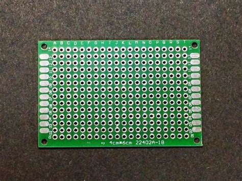
A PCB prototype is a physical representation of the designed circuit board. It is created using the same materials and manufacturing processes as the final product but on a smaller scale. The prototype allows designers to test the functionality, performance, and reliability of the circuit board before mass production.
Why are PCB Prototypes Important?
PCB prototypes are essential for several reasons:
-
Design Validation: Prototypes allow designers to validate their designs and ensure that the circuit board functions as intended.
-
Testing: Prototypes enable thorough testing of the circuit board’s performance, including signal integrity, power consumption, and thermal management.
-
Debugging: If issues arise during testing, prototypes make it easier to identify and fix problems before moving to full-scale production.
-
Cost Savings: By identifying and addressing issues early in the development process, PCB prototypes can help avoid costly mistakes and rework during mass production.
Factors to Consider When Choosing a PCB Prototype
When selecting a suitable PCB prototype for your project, there are several key factors to consider:
1. Material Selection
The choice of material for your PCB prototype is crucial as it affects the board’s performance, durability, and cost. The most common materials used for PCB prototypes are:
-
FR-4: A glass-reinforced epoxy laminate, FR-4 is the most widely used material for PCBs due to its good electrical insulation properties, mechanical strength, and cost-effectiveness.
-
High-Frequency Materials: For high-speed and high-frequency applications, materials like Rogers, Teflon, and PTFE offer superior dielectric properties and low loss at higher frequencies.
-
Flexible Materials: Flexible PCB materials, such as polyimide and PET, are used for applications that require the circuit board to bend or flex.
2. Number of Layers
The number of layers in your PCB prototype depends on the complexity of your design and the required functionality. Single-layer and double-layer PCBs are suitable for simple designs, while multi-layer PCBs (4, 6, 8, or more layers) are used for more complex circuits with higher component density and signal routing requirements.
| Number of Layers | Application |
|---|---|
| Single-layer | Simple, low-cost designs |
| Double-layer | Most common for low to medium complexity |
| 4-layer | Complex designs with moderate signal routing |
| 6-layer or more | High-density, high-speed, and complex designs |
3. Manufacturing Process
The manufacturing process for your PCB prototype can impact the quality, reliability, and cost of the final product. The two main manufacturing processes are:
-
Traditional PCB Fabrication: This process involves etching the circuit pattern onto copper-clad laminates using photolithography and chemical etching. It is suitable for most PCB prototypes and offers good accuracy and reliability.
-
PCB Milling: This process uses a CNC machine to mill the circuit pattern directly onto the copper-clad laminate. It is faster and more cost-effective for small quantities but may have limitations in terms of minimum feature size and accuracy.
4. Surface Finish
The surface finish of your PCB prototype affects the solderability, durability, and appearance of the board. Common surface finishes include:
-
HASL (Hot Air Solder Leveling): A tin-lead alloy is applied to the copper pads and then leveled using hot air. HASL is cost-effective and provides good solderability.
-
ENIG (Electroless Nickel Immersion Gold): A layer of nickel is deposited onto the copper pads, followed by a thin layer of gold. ENIG offers excellent solderability, durability, and shelf life.
-
OSP (Organic Solderability Preservative): A thin, organic coating is applied to the copper pads to prevent oxidation and maintain solderability. OSP is cost-effective and suitable for most applications.
5. Design for Manufacturing (DFM)
When designing your PCB prototype, it is essential to consider the manufacturability of the design. Design for Manufacturing (DFM) guidelines help ensure that your prototype can be efficiently and reliably manufactured. Some key DFM considerations include:
-
Minimum Feature Size: Ensure that your design adheres to the minimum trace width, spacing, and hole size specified by your manufacturer.
-
Pad and Via Size: Use appropriate pad and via sizes to ensure good solderability and reliability.
-
Component Placement: Place components in a way that facilitates easy assembly and minimizes the risk of manufacturing defects.
-
Panelization: If your design will be panelized for mass production, consider the panelization requirements during the prototyping stage.
PCB Prototype Assembly
Once your PCB prototype has been fabricated, the next step is to assemble the components onto the board. There are two main methods for PCB prototype assembly:
1. Hand Assembly
For small quantities and simple designs, hand assembly can be a cost-effective option. This process involves manually soldering the components onto the PCB using a soldering iron. Hand assembly is suitable for through-hole components and can be done in-house or by a small-scale assembly service.
2. Machine Assembly
For larger quantities or more complex designs, machine assembly is recommended. This process uses automated pick-and-place machines to place surface-mount components onto the PCB, followed by a reflow soldering process. Machine assembly offers higher accuracy, consistency, and throughput compared to hand assembly.
When choosing an assembly method for your PCB prototype, consider the following factors:
-
Quantity: For small quantities (typically less than 100 units), hand assembly may be more cost-effective. For larger quantities, machine assembly is usually more efficient.
-
Component Types: Through-hole components are well-suited for hand assembly, while surface-mount components are better suited for machine assembly.
-
Design Complexity: Simple designs with fewer components can be easily hand-assembled, while complex designs with high component density are better suited for machine assembly.
-
Time and Cost: Hand assembly is generally slower and more labor-intensive than machine assembly, but it may be more cost-effective for small quantities. Machine assembly has higher setup costs but offers faster turnaround times and lower per-unit costs for larger quantities.

Testing and Validation
After assembling your PCB prototype, it is crucial to thoroughly test and validate its functionality, performance, and reliability. Some common testing methods include:
1. Visual Inspection
A visual inspection of the assembled PCB prototype can help identify any obvious manufacturing defects, such as bridged solder joints, missing components, or incorrect component placement.
2. Continuity Testing
Continuity testing verifies that the electrical connections between components are intact and that there are no short circuits or open connections. This can be done using a multimeter or a dedicated continuity tester.
3. Functional Testing
Functional testing involves powering up the PCB prototype and verifying that it performs the intended functions correctly. This may include testing input/output signals, communication interfaces, and user interfaces.
4. Environmental Testing
Depending on the intended application, your PCB prototype may need to undergo environmental testing to ensure that it can withstand the expected operating conditions. This may include temperature cycling, humidity testing, vibration testing, and electromagnetic compatibility (EMC) testing.
Frequently Asked Questions (FAQ)
-
Q: How long does it take to manufacture a PCB prototype?
A: The turnaround time for PCB prototype manufacturing varies depending on the complexity of the design, the chosen manufacturing process, and the manufacturer’s workload. Typically, PCB prototypes can be fabricated within 1-2 weeks, but expedited services may be available for faster turnaround times. -
Q: How much does a PCB prototype cost?
A: The cost of a PCB prototype depends on several factors, including the size of the board, the number of layers, the material selection, and the quantity ordered. Small, simple PCB prototypes can cost as little as a few dollars per unit, while larger, more complex designs can cost several hundred dollars or more. Many manufacturers offer discounts for larger quantities. -
Q: Can I manufacture my PCB prototype in-house?
A: Yes, it is possible to manufacture PCB prototypes in-house using a PCB milling machine or a small-scale etching setup. However, this requires an investment in equipment and materials, as well as the necessary skills and knowledge to operate the equipment safely and effectively. For most businesses, outsourcing PCB prototype manufacturing to a specialized service provider is more cost-effective and efficient. -
Q: What files do I need to provide to the manufacturer for PCB prototype fabrication?
A: To fabricate your PCB prototype, you will typically need to provide the manufacturer with a set of Gerber files, which include the copper layer layouts, solder mask, silk screen, and drill files. Additionally, you may need to provide a bill of materials (BOM) and assembly drawings for the prototype assembly process. -
Q: Can I use my PCB prototype for full-scale production?
A: While PCB prototypes are designed to closely resemble the final product, they may not be suitable for full-scale production without further optimization. Based on the feedback and results from prototype testing, you may need to make design changes to improve manufacturability, reliability, or cost-effectiveness before moving to mass production.
Conclusion
Selecting the suitable PCB prototype for your project is essential for successful product development. By considering factors such as material selection, number of layers, manufacturing process, surface finish, and design for manufacturability, you can create a prototype that accurately represents your design intent and enables thorough testing and validation.
When it comes to PCB prototype assembly, choosing between hand assembly and machine assembly depends on the quantity, component types, design complexity, and time and cost constraints of your project.
Thorough testing and validation of your PCB prototype, including visual inspection, continuity testing, functional testing, and environmental testing, help identify and address any issues before moving to full-scale production.
By following best practices and working with experienced PCB prototype manufacturing and assembly partners, you can ensure that your PCB prototype meets your requirements and sets the stage for a successful final product.
Leave a Reply