Introduction to PCB Prototyping
PCB prototyping is an essential part of the electronics design process, allowing engineers and makers to test and refine their designs before committing to mass production. In this article, we’ll explore the importance of quick turn and fast PCB prototyping, the various methods available, and tips for achieving the best results.
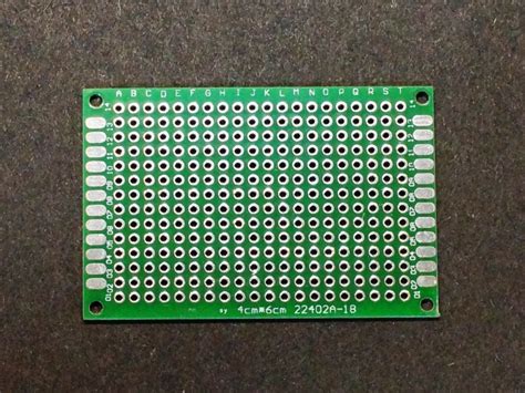
What is a PCB Prototype?
A PCB prototype is a physical representation of a printed circuit board design, used for testing and validation purposes. It allows designers to:
- Verify the functionality of their circuit design
- Test the physical layout and component placement
- Identify and resolve any issues before mass production
Benefits of Quick Turn and Fast PCB Prototyping
Quick turn and fast PCB prototyping offer several advantages for engineers and makers:
- Reduced time-to-market
- Lower development costs
- Increased design flexibility
- Early identification of design flaws
PCB Prototyping Methods
There are several methods available for creating PCB prototypes, each with its own advantages and disadvantages.
Traditional PCB Fabrication
Traditional PCB fabrication involves the following steps:
- Design the PCB using EDA software
- Generate Gerber files
- Send files to a PCB manufacturer
- Wait for the prototype to be fabricated and shipped
While this method offers high-quality results, it can be time-consuming and expensive for small quantities.
In-House PCB Milling
In-house PCB milling uses a desktop CNC machine to mill the copper traces directly onto a blank PCB substrate. This method offers several advantages:
- Quick turnaround times
- Low cost for small quantities
- Ability to make design changes on-the-fly
However, the quality and complexity of the PCBs may be limited compared to traditional fabrication methods.
PCB Prototyping Services
PCB prototyping services offer a balance between the speed of in-house milling and the quality of traditional fabrication. These services typically offer:
- Online PCB design tools
- Quick turnaround times (as fast as 24 hours)
- Affordable pricing for small quantities
- High-quality fabrication
Some popular PCB prototyping services include:
| Service | Turnaround Time | Minimum Quantity | Price (10x10cm, 2 layers) |
|---|---|---|---|
| PCBWay | 24 hours | 5 | $5 |
| JLCPCB | 24 hours | 5 | $2 |
| OSH Park | 5-12 days | 3 | $5 per square inch |

Designing for Quick Turn and Fast PCB Prototyping
To ensure the best results when using quick turn and fast PCB prototyping services, follow these design tips:
Keep the Design Simple
- Use larger components and wider trace widths
- Avoid complex layouts and high-density designs
- Stick to standard PCB sizes and shapes
Use Standard Components
- Choose components that are readily available
- Avoid using obsolete or hard-to-find components
- Use surface-mount components whenever possible
Follow the Manufacturer’s Design Guidelines
- Adhere to the minimum trace width and spacing requirements
- Use the recommended solder mask and silkscreen colors
- Follow the manufacturer’s file submission guidelines
Test and Validate the Design
- Use EDA software to perform design rule checks (DRC)
- Verify the functionality of the circuit through simulation
- Double-check the component footprints and pinouts

Case Studies
Case Study 1: Rapid Prototyping for Wearable Electronics
A startup company developing a new wearable device needed to quickly iterate on their PCB design to meet a tight product launch deadline. By using a quick turn PCB prototyping service, they were able to:
- Receive prototypes within 48 hours of submitting their design
- Test and refine the design over multiple iterations
- Finalize the design and move to mass production in less than a month
Case Study 2: Cost-Effective Prototyping for Hobby Projects
A hobbyist working on a DIY Arduino-based robot wanted to create custom PCBs for the project without breaking the bank. By using an in-house PCB milling machine, they were able to:
- Create PCB prototypes for less than $10 in materials
- Quickly modify the design and create new prototypes as needed
- Successfully complete the project and share it with the maker community

Frequently Asked Questions (FAQ)
1. How much does it cost to prototype a PCB?
The cost of prototyping a PCB varies depending on the method used, the size and complexity of the design, and the quantity required. In-house milling can cost as little as a few dollars in materials, while PCB prototyping services typically charge $2 to $10 per board for small quantities.
2. How long does it take to receive a PCB prototype?
The turnaround time for PCB prototypes depends on the method used. In-house milling can produce prototypes in a matter of hours, while traditional fabrication can take several weeks. PCB prototyping services offer the fastest turnaround times, with some providing prototypes in as little as 24 hours.
3. What is the minimum quantity for PCB prototyping?
The minimum quantity for PCB prototyping varies by method and manufacturer. In-house milling has no minimum quantity, while traditional fabrication often requires a minimum of 100 or more boards. PCB prototyping services typically have a minimum quantity of 5 to 10 boards.
4. Can I use any EDA software for PCB prototyping?
Most PCB prototyping services and manufacturers accept design files from popular EDA software packages such as Altium, Eagle, and KiCad. However, it’s essential to check with the specific service or manufacturer for their file submission guidelines and supported software.
5. What are the limitations of quick turn and fast PCB prototyping?
Quick turn and fast PCB prototyping methods may have limitations in terms of the complexity and density of the designs they can accommodate. High-speed designs, tight trace spacing, and advanced features like buried vias may not be suitable for these methods. It’s essential to consider the specific requirements of your design when choosing a prototyping method.
Conclusion
Quick turn and fast PCB prototyping are invaluable tools for engineers and makers looking to bring their electronic designs to life quickly and efficiently. By understanding the various methods available and following best practices for design and manufacturing, you can take advantage of these services to accelerate your development process and create successful products.


Leave a Reply