Introduction to Laser PCB Technology
The printed circuit board (PCB) manufacturing industry has seen significant advancements in recent years, with laser technology playing a crucial role in improving efficiency and precision. Laser exposure machines have revolutionized the way PCBs are fabricated, offering numerous benefits over traditional methods. In this article, we will explore the world of laser PCB technology and how it is transforming the electronics industry.
What is a Laser Exposure Machine?
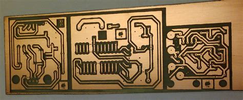
A laser exposure machine is a sophisticated device that uses high-precision lasers to transfer the circuit pattern onto the photoresist layer of a PCB. Unlike conventional exposure methods that rely on UV light and photomasks, laser exposure machines directly write the circuit pattern using a focused laser beam. This direct imaging approach eliminates the need for physical photomasks, reducing costs and increasing flexibility in PCB design.

How Laser Exposure Machines Work
The process of creating a PCB using a laser exposure machine involves several key steps:
-
PCB Design: The circuit design is created using specialized software, such as Altium Designer or KiCad. The design file is then converted into a format compatible with the laser exposure machine.
-
Photoresist Application: The PCB substrate is coated with a light-sensitive photoresist material, which hardens when exposed to light.
-
Laser Exposure: The PCB is placed in the laser exposure machine, where a high-precision laser beam scans the surface, selectively exposing the photoresist according to the circuit pattern. The laser beam is controlled by a computer-aided manufacturing (CAM) system that ensures accurate and consistent results.
-
Development: After exposure, the PCB is subjected to a development process, where the exposed photoresist is removed, leaving behind the desired circuit pattern.
-
Etching: The developed PCB undergoes an etching process, where the unwanted copper is removed, leaving only the circuit traces.
-
Finishing: The PCB is then subjected to various finishing processes, such as solder mask application, silkscreen printing, and surface finishing, to enhance its durability and performance.

Benefits of Laser PCB Technology
Laser exposure machines offer several compelling advantages over traditional PCB manufacturing methods:
-
Higher Precision: Laser exposure machines can achieve much higher resolutions compared to conventional methods. They can produce circuit features as small as 25 microns, enabling the fabrication of high-density PCBs with intricate designs.
-
Faster Turnaround: With laser exposure machines, the time-consuming process of creating and aligning photomasks is eliminated. This results in faster turnaround times, allowing manufacturers to respond quickly to customer demands and bring products to market faster.
-
Cost Savings: The elimination of photomasks reduces material costs and minimizes the need for expensive tooling. Additionally, the increased precision and faster production times lead to overall cost savings in the PCB manufacturing process.
-
Design Flexibility: Laser exposure machines enable greater design flexibility, as they can easily accommodate changes in circuit patterns without requiring new photomasks. This flexibility is particularly valuable for prototyping and low-volume production runs.
-
Improved Reliability: The high precision and consistency achieved by laser exposure machines result in PCBs with improved reliability and performance. The accurate placement of circuit features reduces the risk of defects and ensures optimal signal integrity.

Applications of Laser PCB Technology
Laser PCB technology finds applications in various industries and sectors:
-
Consumer Electronics: Laser exposure machines are extensively used in the production of PCBs for smartphones, tablets, laptops, and other consumer electronic devices. The high precision and miniaturization capabilities of laser technology enable the fabrication of compact and feature-rich PCBs.
-
Automotive Industry: Modern vehicles rely heavily on electronic systems for functions such as engine control, infotainment, and advanced driver assistance systems (ADAS). Laser PCB technology is crucial for producing reliable and high-performance PCBs that can withstand the harsh automotive environment.
-
Medical Devices: Medical devices, such as implantable sensors, diagnostic equipment, and wearable health monitors, require PCBs with high precision and reliability. Laser exposure machines are essential for manufacturing PCBs that meet the stringent requirements of the medical industry.
-
Aerospace and Defense: PCBs used in aerospace and defense applications must withstand extreme conditions and meet rigorous performance standards. Laser PCB technology enables the production of high-reliability PCBs that can operate in harsh environments and meet the demands of mission-critical systems.
-
Industrial Automation: The increasing adoption of automation and Industry 4.0 technologies has driven the demand for advanced PCBs in industrial settings. Laser exposure machines play a vital role in producing PCBs for industrial control systems, sensors, and communication devices.
Laser PCB Market and Industry Trends
The laser PCB market has experienced significant growth in recent years, driven by the increasing demand for high-performance and miniaturized electronic devices. According to a market research report, the global laser PCB market is expected to reach USD 1.2 billion by 2025, growing at a CAGR of 5.8% during the forecast period (2020-2025).
| Region | Market Share (2020) | CAGR (2020-2025) |
|---|---|---|
| North America | 35% | 5.5% |
| Europe | 30% | 5.2% |
| Asia-Pacific | 25% | 6.5% |
| Rest of World | 10% | 5.0% |
Several industry trends are shaping the future of laser PCB technology:
-
Miniaturization: The demand for smaller and more compact electronic devices is driving the need for high-density PCBs with fine pitch features. Laser exposure machines are essential for achieving the required miniaturization and precision.
-
5G and IoT: The deployment of 5G networks and the growth of the Internet of Things (IoT) are creating new opportunities for laser PCB technology. The high-frequency and high-speed requirements of 5G and IoT devices necessitate PCBs with superior signal integrity and reliability, which can be achieved through laser exposure machines.
-
Sustainable Manufacturing: There is a growing emphasis on sustainable and eco-friendly manufacturing practices in the PCB industry. Laser exposure machines contribute to sustainability by reducing material waste, eliminating the need for harmful chemicals, and enabling more efficient production processes.
-
Advanced Materials: The development of advanced PCB materials, such as high-frequency laminates and flexible substrates, is driving the adoption of laser exposure machines. These machines are capable of handling diverse materials and enabling the fabrication of cutting-edge PCBs.
Frequently Asked Questions (FAQ)
1. What is the difference between laser exposure and traditional UV exposure in PCB manufacturing?
Laser exposure machines use a focused laser beam to directly write the circuit pattern onto the photoresist layer of the PCB. In contrast, traditional UV exposure methods rely on a photomask and UV light to transfer the pattern. Laser exposure offers higher precision, eliminates the need for photomasks, and enables faster turnaround times.
2. Can laser exposure machines handle multi-layer PCBs?
Yes, laser exposure machines are capable of handling multi-layer PCBs. They can accurately align and expose each layer, ensuring precise registration and minimizing the risk of misalignment or defects.
3. What are the limitations of laser PCB technology?
While laser PCB technology offers numerous benefits, it does have some limitations. The initial investment in laser exposure machines can be high, making it more suitable for high-volume production. Additionally, laser exposure may not be cost-effective for very large PCBs or extremely complex designs.
4. How does laser PCB technology compare to inkjet printing for PCB Prototyping?
Laser PCB technology and inkjet printing are both viable options for PCB prototyping. Inkjet printing offers the advantage of being able to directly print conductive traces onto the PCB substrate, making it suitable for rapid prototyping. However, laser exposure machines provide higher precision and can handle more complex designs, making them a preferred choice for high-quality prototypes.
5. What is the future outlook for laser PCB technology?
The future of laser PCB technology looks promising, driven by the increasing demand for high-performance and miniaturized electronic devices. As the electronics industry continues to evolve, laser exposure machines are expected to play a crucial role in enabling the fabrication of advanced PCBs. Continuous advancements in laser technology, materials science, and manufacturing processes will further enhance the capabilities and adoption of laser PCB technology.
Conclusion
Laser exposure machines have revolutionized the PCB manufacturing industry, offering higher precision, faster turnaround times, and improved efficiency compared to traditional methods. By eliminating the need for photomasks and enabling direct imaging of circuit patterns, laser PCB technology has opened up new possibilities for PCB design and fabrication.
As the demand for high-performance and miniaturized electronic devices continues to grow, laser PCB technology will play a crucial role in meeting the evolving needs of various industries, including consumer electronics, automotive, medical devices, aerospace, and industrial automation.
With ongoing advancements in laser technology, materials science, and manufacturing processes, the future of laser PCB technology looks bright. Manufacturers and designers who embrace this technology will be well-positioned to stay competitive in the rapidly evolving electronics landscape.


Leave a Reply