Introduction
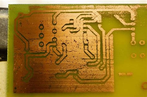
Printed circuit board (PCB) manufacturing is a complex process that involves many steps, including etching. Etching is a critical step in PCB manufacturing that removes unwanted copper from the board to create the desired circuit pattern. However, etching can be challenging, especially in multilayer PCB manufacturing, where multiple layers of copper are laminated together. In this article, we will discuss three common issues of etching in multilayer PCB manufacturing: underetching, overetching, and uneven etching.
What is PCB etching?
PCB etching is the process of removing unwanted copper from a PCB to create the desired circuit pattern. The etching process involves applying a chemical solution, known as an etchant, to the copper surface of the PCB. The etchant reacts with the copper, dissolving it and leaving behind the desired circuit pattern.
There are two main types of etching used in PCB manufacturing: subtractive etching and additive etching. Subtractive etching involves removing unwanted copper from a copper-clad board, while additive etching involves adding copper to a bare board to create the desired circuit pattern.
Subtractive Etching
Subtractive etching is the most common type of etching used in PCB manufacturing. It involves the following steps:
- A copper-clad board is coated with a photoresist material.
- The photoresist is exposed to light through a photomask, which contains the desired circuit pattern.
- The exposed photoresist is developed, leaving behind a pattern of exposed copper.
- The board is immersed in an etchant solution, which removes the exposed copper.
- The remaining photoresist is removed, leaving behind the desired circuit pattern.
Additive Etching
Additive etching is a less common type of etching used in PCB manufacturing. It involves the following steps:
- A bare board is coated with a seed layer of copper.
- A photoresist material is applied to the board and exposed to light through a photomask.
- The exposed photoresist is developed, leaving behind a pattern of exposed copper.
- Additional copper is electroplated onto the exposed copper to create the desired circuit pattern.
- The remaining photoresist is removed, leaving behind the desired circuit pattern.

Issue 1: Underetching
Underetching is a common issue in multilayer PCB manufacturing where the etchant fails to remove all of the unwanted copper from the board. This can result in short circuits, poor electrical performance, and reduced reliability of the PCB.
Causes of Underetching
There are several causes of underetching in multilayer PCB manufacturing, including:
- Insufficient etchant concentration
- Incorrect etchant temperature
- Insufficient etching time
- Contamination of the etchant solution
- Poor quality copper foil
Solutions for Underetching
To prevent underetching in multilayer PCB manufacturing, the following solutions can be implemented:
- Ensure the etchant concentration is correct and consistent
- Maintain the etchant temperature within the recommended range
- Increase the etching time to ensure complete removal of unwanted copper
- Regularly monitor and maintain the etchant solution to prevent contamination
- Use high-quality copper foil with consistent thickness and surface finish

Issue 2: Overetching
Overetching is another common issue in multilayer PCB manufacturing where the etchant removes too much copper from the board, resulting in damaged or missing traces, pads, or vias. This can lead to open circuits, poor electrical performance, and reduced reliability of the PCB.
Causes of Overetching
There are several causes of overetching in multilayer PCB manufacturing, including:
- Excessive etchant concentration
- Incorrect etchant temperature
- Excessive etching time
- Poor quality photoresist or photomask
- Inconsistent copper thickness
Solutions for Overetching
To prevent overetching in multilayer PCB manufacturing, the following solutions can be implemented:
- Ensure the etchant concentration is correct and consistent
- Maintain the etchant temperature within the recommended range
- Reduce the etching time to prevent excessive removal of copper
- Use high-quality photoresist and photomasks with consistent thickness and resolution
- Use copper foil with consistent thickness and surface finish

Issue 3: Uneven Etching
Uneven etching is a common issue in multilayer PCB manufacturing where the etchant removes copper unevenly across the board, resulting in inconsistent trace widths, impedance mismatches, and signal integrity issues. This can lead to poor electrical performance and reduced reliability of the PCB.
Causes of Uneven Etching
There are several causes of uneven etching in multilayer PCB manufacturing, including:
- Inconsistent etchant flow or agitation
- Uneven copper thickness or surface finish
- Poor quality photoresist or photomask
- Inconsistent lamination or bonding of layers
- Mechanical stress or damage during handling
Solutions for Uneven Etching
To prevent uneven etching in multilayer PCB manufacturing, the following solutions can be implemented:
- Ensure consistent and uniform etchant flow and agitation across the board
- Use copper foil with consistent thickness and surface finish
- Use high-quality photoresist and photomasks with consistent thickness and resolution
- Ensure consistent lamination and bonding of layers to prevent delamination or warping
- Handle boards carefully to prevent mechanical stress or damage
FAQ
- What is the difference between subtractive and additive etching?
-
Subtractive etching involves removing unwanted copper from a copper-clad board, while additive etching involves adding copper to a bare board to create the desired circuit pattern.
-
What are the most common causes of underetching in multilayer PCB manufacturing?
-
The most common causes of underetching in multilayer PCB manufacturing are insufficient etchant concentration, incorrect etchant temperature, insufficient etching time, contamination of the etchant solution, and poor quality copper foil.
-
How can overetching be prevented in multilayer PCB manufacturing?
-
Overetching can be prevented in multilayer PCB manufacturing by ensuring the etchant concentration is correct and consistent, maintaining the etchant temperature within the recommended range, reducing the etching time to prevent excessive removal of copper, using high-quality photoresist and photomasks with consistent thickness and resolution, and using copper foil with consistent thickness and surface finish.
-
What are the consequences of uneven etching in multilayer PCB manufacturing?
-
Uneven etching in multilayer PCB manufacturing can result in inconsistent trace widths, impedance mismatches, and signal integrity issues, leading to poor electrical performance and reduced reliability of the PCB.
-
How can uneven etching be prevented in multilayer PCB manufacturing?
- Uneven etching can be prevented in multilayer PCB manufacturing by ensuring consistent and uniform etchant flow and agitation across the board, using copper foil with consistent thickness and surface finish, using high-quality photoresist and photomasks with consistent thickness and resolution, ensuring consistent lamination and bonding of layers to prevent delamination or warping, and handling boards carefully to prevent mechanical stress or damage.
Conclusion
Etching is a critical step in multilayer PCB manufacturing that can significantly impact the quality and reliability of the final product. Underetching, overetching, and uneven etching are three common issues that can occur during the etching process, leading to short circuits, open circuits, impedance mismatches, and signal integrity issues.
To prevent these issues, it is essential to carefully control the etching process parameters, such as etchant concentration, temperature, and time, and to use high-quality materials and equipment. Regular monitoring and maintenance of the etching process and equipment can also help to prevent issues and ensure consistent results.
By understanding the causes and solutions for common etching issues in multilayer PCB manufacturing, PCB manufacturers can optimize their processes and produce high-quality, reliable PCBs that meet the demanding requirements of today’s electronic devices.


Leave a Reply