What is PCB Stackup?
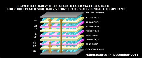
PCB stackup refers to the arrangement of copper and insulating layers in a printed circuit board (PCB). It is a critical aspect of PCB Design, as it determines the board’s electrical properties, mechanical strength, and manufacturability. A well-designed PCB stackup ensures proper signal integrity, reduces electromagnetic interference (EMI), and minimizes manufacturing issues.
Key Components of a PCB Stackup
- Copper Layers:
- Signal layers: Used for routing traces and connecting components
- Power and ground planes: Provide stable voltage references and return paths for signals
- Dielectric Layers:
- Insulating material between copper layers, typically FR-4 or other laminate materials
- Solder Mask:
- Protective coating applied to the outer layers to prevent oxidation and provide insulation
- Silkscreen:
- Text and symbols printed on the solder mask for component identification and assembly guidance
Factors to Consider When Designing a PCB Stackup
1. Board Thickness
The overall thickness of the PCB is determined by the number of layers and the thickness of each layer. Thicker boards provide better mechanical stability but may increase manufacturing costs. Common board thicknesses range from 0.8mm to 2.4mm.
2. Layer Count
The number of layers in a PCB stackup depends on the complexity of the design and the required functionality. Higher layer counts allow for more routing options and better signal integrity but also increase manufacturing costs.
| Layer Count | Typical Applications |
|---|---|
| 1-2 | Simple designs, low-cost applications |
| 4 | Common for most designs, good balance |
| 6-8 | Complex designs, high-speed applications |
| 10+ | Very complex designs, high-density boards |
3. Material Selection
The choice of dielectric material significantly impacts the electrical and mechanical properties of the PCB. The most common material is FR-4, which offers good performance and cost-effectiveness. Other materials, such as Rogers or Isola, may be used for high-frequency or high-speed applications.
| Material | Dielectric Constant | Loss Tangent | Applications |
|---|---|---|---|
| FR-4 | 4.3-4.7 | 0.02 | General-purpose, cost-effective |
| Rogers | 2.2-10.2 | 0.0009-0.003 | High-frequency, low-loss |
| Isola | 3.0-3.7 | 0.004-0.02 | High-speed, low-loss |
4. Impedance Control
Maintaining proper impedance throughout the PCB is crucial for signal integrity and reducing reflections. The stackup design should consider the required impedance for various signal types, such as single-ended, differential pairs, or controlled impedance traces.
Common Impedance Values
- Single-ended traces: 50Ω or 75Ω
- Differential pairs: 90Ω or 100Ω
- USB: 90Ω differential
5. Via Types and Placement
Vias are used to connect traces between layers in a PCB stackup. The type and placement of vias can affect signal integrity and manufacturability.
Via Types
- Through-hole vias: Connect all layers, may cause signal integrity issues
- Blind vias: Connect outer layers to inner layers, better signal integrity
- Buried vias: Connect inner layers only, best signal integrity but higher cost
Via Placement
- Avoid placing vias in high-speed or sensitive signal paths
- Minimize via stubs to reduce reflections and signal distortion
- Use via-in-pad for high-density designs
6. Copper Weight and Trace Width
The copper weight and trace width affect the current-carrying capacity and impedance of the traces. Thicker copper allows for higher current but may increase manufacturing costs. Trace width should be selected based on the required impedance and current-carrying capacity.
Common Copper Weights
- 0.5 oz/ft² (17 µm): Low-current applications, low-cost
- 1 oz/ft² (35 µm): General-purpose, most common
- 2 oz/ft² (70 µm): High-current applications, power planes
- 3 oz/ft² (105 µm): Very high-current applications, specialty designs
7. Shielding and Grounding
Proper shielding and grounding techniques help reduce EMI and ensure signal integrity. Some strategies include:
- Using dedicated ground planes for each signal layer
- Implementing ground stitching vias to provide low-impedance return paths
- Incorporating shielding layers or guard traces for sensitive signals
- Separating analog and digital ground planes to minimize noise coupling
PCB Stackup Design Process
- Determine the required board thickness and layer count based on the design complexity and manufacturing constraints
- Select appropriate dielectric materials for the desired electrical and mechanical properties
- Define the copper weight and trace width for each layer based on the required impedance and current-carrying capacity
- Assign signal, power, and ground layers to maintain proper shielding and grounding
- Place vias strategically to minimize signal integrity issues and improve manufacturability
- Verify the stackup design using PCB Layout software and manufacturer feedback
- Iterate and refine the stackup as needed to meet design requirements and manufacturing constraints

Best Practices for PCB Stackup Design
- Keep the stackup symmetrical to minimize warping and mechanical stress
- Use a consistent dielectric thickness between layers to maintain impedance control
- Avoid placing signal layers adjacent to each other to reduce crosstalk
- Use a minimum of two ground planes for better shielding and signal integrity
- Route high-speed signals on inner layers to minimize EMI and crosstalk
- Follow manufacturer guidelines for minimum trace width, spacing, and via sizes
- Document the stackup clearly, including layer assignments, materials, and copper weights
Frequently Asked Questions (FAQ)
1. What is the most common PCB stackup for a 4-layer board?
A typical 4-layer PCB stackup consists of:
– Layer 1: Signal
– Layer 2: Ground
– Layer 3: Power
– Layer 4: Signal
This arrangement provides good signal integrity and shielding while minimizing manufacturing costs.
2. Can I use different dielectric materials in the same PCB stackup?
Yes, it is possible to use different dielectric materials in the same PCB stackup. This is known as a hybrid stackup and can be used to optimize the electrical and mechanical properties of specific layers. However, it may increase manufacturing complexity and costs.
3. How do I determine the appropriate trace width for my PCB stackup?
The appropriate trace width depends on several factors, including the required impedance, current-carrying capacity, and the PCB manufacturer’s capabilities. You can use PCB design software or online calculators to determine the trace width based on these factors. It’s essential to consult with your PCB manufacturer to ensure that your chosen trace width is within their manufacturing capabilities.
4. What is the difference between blind and buried vias?
Blind vias connect an outer layer to one or more inner layers, but do not go through the entire board. Buried vias, on the other hand, connect inner layers only and are not visible from the outer layers. Blind vias offer better signal integrity than through-hole vias, while buried vias provide the best signal integrity but come with higher manufacturing costs.
5. How can I reduce EMI in my PCB stackup?
To reduce EMI in your PCB stackup, you can:
1. Use dedicated ground planes for each signal layer
2. Implement ground stitching vias to provide low-impedance return paths
3. Incorporate shielding layers or guard traces for sensitive signals
4. Separate analog and digital ground planes to minimize noise coupling
5. Route high-speed signals on inner layers to minimize radiation
By following these guidelines and best practices, you can design a PCB stackup that ensures proper signal integrity, reduces EMI, and meets your specific design requirements while minimizing manufacturing costs and complexity.
Leave a Reply