Introduction to PCB Buildup
Printed Circuit Boards (PCBs) are essential components in modern electronics. They provide a platform for mounting and interconnecting electronic components, enabling the creation of complex circuits. The buildup of a PCB refers to the layered structure of the board, which consists of conductive and insulating materials. Understanding the PCB buildup is crucial for designers and manufacturers to ensure the proper functioning and reliability of electronic devices.
Key Components of PCB Buildup
- Substrate material
- Copper layers
- Solder mask
- Silkscreen
- Surface finish
PCB Substrate Materials
The substrate is the foundation of a PCB, providing mechanical support and electrical insulation. The choice of substrate material depends on the application, cost, and performance requirements.
Common PCB Substrate Materials
| Material | Description | Applications |
|---|---|---|
| FR-4 | Fiberglass-reinforced epoxy laminate | General-purpose, high-volume production |
| Polyimide | High-temperature resistant polymer | Aerospace, military, high-reliability applications |
| Ceramic | Aluminum oxide or aluminum nitride | High-frequency, high-power, and high-temperature applications |
| Metal Core | Aluminum or copper base with dielectric layer | High-power LED lighting, automotive, and power electronics |

Copper Layers in PCB Buildup
Copper layers are the conductive pathways that carry electrical signals and power throughout the PCB. The number and arrangement of copper layers determine the complexity and functionality of the board.
Types of Copper Layers
- Signal Layers
- Used for routing electrical signals between components
- Typically outer layers (top and bottom) for single- or double-sided boards
- Inner layers for multi-layer boards
- Power and Ground Planes
- Provide stable power distribution and reference voltages
- Usually inner layers in multi-layer boards
- Help reduce electromagnetic interference (EMI) and improve signal integrity
Copper Thickness and Weight
Copper thickness is expressed in ounces per square foot (oz/ft²) or microns (µm). Common copper weights include:
– 0.5 oz/ft² (17.5 µm)
– 1 oz/ft² (35 µm)
– 2 oz/ft² (70 µm)
– 3 oz/ft² (105 µm)
Thicker copper layers are used for high-current applications or to improve thermal dissipation.

Solder Mask in PCB Buildup
Solder mask is a protective coating applied to the copper layers of a PCB. It serves several purposes:
1. Insulates and protects the copper traces from oxidation and contamination
2. Prevents solder bridging between closely spaced pads during assembly
3. Provides a surface for applying component designators and other markings
4. Enhances the aesthetics of the PCB
Solder Mask Colors
Solder mask is available in various colors, with green being the most common. Other popular colors include:
– Red
– Blue
– Black
– White
– Yellow
The choice of solder mask color is usually based on aesthetic preferences or to improve visibility for automated optical inspection (AOI) systems.

Silkscreen in PCB Buildup
Silkscreen, also known as legend or nomenclature, is a printed layer on top of the solder mask that provides human-readable information about the PCB and its components. This information includes:
– Component designators (e.g., R1, C2, U3)
– Polarity indicators (e.g., + and – symbols)
– Test points
– Company logos or product branding
– Regulatory markings (e.g., UL, CE, RoHS)
Silkscreen is typically printed in white ink, but other colors such as black or yellow can be used for improved contrast or aesthetic reasons.
Surface Finish in PCB Buildup
The surface finish is the final metallic coating applied to the exposed copper pads and vias of a PCB. It serves several purposes:
1. Protects the copper from oxidation and corrosion
2. Enhances solderability during component assembly
3. Improves electrical conductivity and contact reliability
4. Provides a surface for wire bonding or other specialized assembly techniques
Common Surface Finishes
| Finish | Description | Applications |
|---|---|---|
| HASL (Hot Air Solder Leveling) | Tin-lead alloy coating | General-purpose, low-cost |
| ENIG (Electroless Nickel Immersion Gold) | Nickel layer with thin gold coating | High-reliability, long shelf life, wire bonding |
| ENEPIG (Electroless Nickel Electroless Palladium Immersion Gold) | Nickel, palladium, and gold layers | High-frequency, fine-pitch, and press-fit connectors |
| OSP (Organic Solderability Preservative) | Organic compound coating | Low-cost, flat surface, short shelf life |
| Immersion Silver | Thin silver coating | Low-cost, high-conductivity, short shelf life |
| Immersion Tin | Thin tin coating | Lead-free, cost-effective, flat surface |
The choice of surface finish depends on the application requirements, component types, assembly processes, and cost considerations.
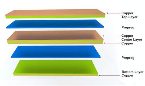
Multi-Layer PCB Buildup
Multi-layer PCBs consist of multiple copper layers separated by insulating material, allowing for more complex routing and higher component density. The buildup of a multi-layer PCB involves several steps:
- Core Construction
- A pre-fabricated, double-sided copper-clad laminate serves as the core of the multi-layer PCB
- The core is patterned and etched to create the inner copper layers
-
Vias are drilled and plated to interconnect the inner layers
-
Layer Stacking
- Additional copper layers are added to the top and bottom of the core using a lamination process
- Pre-impregnated (prepreg) fiberglass sheets are placed between the layers as insulation
-
The stack is subjected to heat and pressure to bond the layers together
-
Outer Layer Processing
- The outer copper layers are patterned and etched to create the final circuit layout
- Solder mask and silkscreen are applied to the outer layers
-
Surface finish is applied to the exposed copper areas
-
Final Fabrication
- The multi-layer PCB panel is drilled to create through-holes and mounting holes
- The panel is cut or routed to separate individual PCBs
- Electrical testing and quality inspection are performed
Advanced PCB Buildup Techniques
As electronics become more complex and demanding, advanced PCB buildup techniques have emerged to address specific challenges:
High Density Interconnect (HDI)
- Uses microvias and fine-pitch traces to achieve higher routing density
- Enables smaller form factors and improved signal integrity
- Commonly used in smartphones, wearables, and high-performance computing
Embedded Components
- Discrete components (e.g., resistors, capacitors) are embedded within the PCB Layers
- Reduces surface component count and improves device miniaturization
- Enhances electrical performance and reliability
Rigid-Flex PCBs
- Combines rigid and Flexible PCB sections in a single assembly
- Allows for three-dimensional packaging and improved shock and vibration resistance
- Used in aerospace, medical, and wearable applications
Frequently Asked Questions (FAQ)
-
Q: What is the difference between a single-sided and double-sided PCB?
A: A single-sided PCB has copper traces on only one side of the substrate, while a double-sided PCB has copper traces on both sides. Double-sided PCBs offer more routing flexibility and higher component density compared to single-sided boards. -
Q: How do vias work in a multi-layer PCB?
A: Vias are plated holes that interconnect different copper layers in a multi-layer PCB. They allow signals and power to pass through the layers, enabling more complex routing and component placement. There are several types of vias, including through-hole, blind, and buried vias, each serving specific purposes in the PCB design. -
Q: What is the purpose of a power plane in a PCB?
A: A power plane is a solid copper layer in a multi-layer PCB that is dedicated to distributing power to the components on the board. It provides a low-impedance, low-inductance path for the power supply, minimizing voltage drops and improving power integrity. Power planes also help reduce electromagnetic interference (EMI) by acting as a shield between signal layers. -
Q: How does the choice of surface finish affect the assembly process?
A: The surface finish of a PCB plays a crucial role in the assembly process. It affects the solderability, wettability, and reliability of the solder joints. Different surface finishes have varying characteristics, such as shelf life, flatness, and compatibility with different solder alloys. The choice of surface finish should be based on the specific requirements of the assembly process, component types, and environmental conditions. -
Q: What are the advantages of using embedded components in a PCB?
A: Embedded components offer several advantages over surface-mounted components: - Reduced board size and thickness
- Improved electrical performance due to shorter signal paths
- Enhanced reliability due to reduced solder joints and better protection from environmental factors
- Increased design flexibility and component density
- Potential cost savings in high-volume production
However, the design and manufacturing process for embedded component PCBs is more complex and requires specialized equipment and expertise.
Conclusion
The buildup of a PCB is a critical aspect of electronic product design and manufacturing. It involves the careful selection and arrangement of substrate materials, copper layers, solder mask, silkscreen, and surface finish to create a functional and reliable circuit board. Understanding the various components and techniques used in PCB buildup enables designers to make informed decisions and optimize their designs for specific applications.
As technology advances, the demand for more complex and compact electronic devices drives the development of advanced PCB buildup techniques, such as HDI, embedded components, and Rigid-Flex PCBs. These innovations push the boundaries of PCB design and manufacturing, enabling the creation of ever-more sophisticated and reliable electronic products.
By mastering the fundamentals of PCB buildup and staying up-to-date with the latest advancements in the field, designers and manufacturers can create PCBs that meet the evolving needs of the electronics industry and deliver cutting-edge products to the market.


Leave a Reply