What is QFP Solder Bridging?
QFP (Quad Flat Package) solder bridging is a common defect that occurs when soldering QFP Integrated Circuits to printed circuit boards (PCBs). QFP packages have leads on all four sides of the IC chip. The leads are spaced very close together, typically with a pitch (distance between leads) of 0.5mm or less.
Solder bridging happens when excess solder accidentally connects adjacent leads, causing an unintended short circuit between pins. This bridging of solder prevents the circuit from functioning properly. QFP solder bridges are a frequent issue in PCB Assembly due to the high pin density and small pitch of QFP packages.
Some common causes of QFP solder bridging include:
- Applying too much solder paste
- Incorrect reflow oven temperature profile
- Poor PCB pad design or Solder mask clearance
- Bent or misaligned QFP leads
Solder bridges on QFP packages can be difficult to prevent and rework. However, by following best practices in the PCB design, solder paste printing, and Reflow soldering processes, the incidence of QFP solder bridging can be significantly reduced.
Strategies to Prevent QFP Solder Bridging
Proper PCB Footprint Design
Preventing solder bridges begins with a robust PCB footprint design for the QFP package. The footprint should be designed with sufficient solder mask clearances between pads. Solder mask prevents exposed copper from accepting solder. Having a wide enough solder mask gap between pads prevents solder from bridging between leads.
The pad sizes should also be optimized for the particular QFP package size and pitch. QFP packages are available in a range of body sizes and lead pitches. Consult the package datasheet to determine the ideal pad size.
In general, finer pitch QFPs require smaller pads to maintain adequate solder mask clearances. A typical pad width for a 0.5mm pitch QFP is around 0.25mm. Larger pads invite more solder to the joint, increasing the likelihood of bridging.
Optimize Solder Paste Stencil Design
The next step is to design the solder paste stencil apertures for the QFP footprint. Solder paste is applied to the PCB pads through a laser-cut stencil using a screen printing process. The stencil aperture openings must be precisely sized to apply the optimal amount of paste.
Stencil apertures that are oversized deposit excess paste on the pads, causing solder balling and bridging. Undersized apertures apply insufficient paste, leading to poor wetting and opens. The ideal transfer ratio (area of paste divided by area of pad) is typically between 0.66 to 0.9 for QFPs.
Stencil thickness also impacts the paste volume. Thicker stencils deposit a greater volume of solder paste. A typical stencil thickness for QFPs is 0.1mm (4 mils) to 0.15mm (6 mils).
Consider using home plates on the solder stencil for fine-pitch QFPs. Home plates have enlarged openings at the leads to provide additional paste volume without increasing the printed area and risk of bridging.
Control Solder Paste Printing Process
Consistent solder paste printing is critical for avoiding QFP solder defects. Even with a well-designed stencil, the printing process must be controlled to achieve acceptable paste deposits.
Key factors in the solder paste printing process include:
- Squeegee type and pressure
- Snap-off distance
- Print speed
- Stencil underside cleaning frequency
Metal squeegees provide the most consistent paste deposits for fine feature printing. Squeegee pressure and speed should be optimized to fully clear the apertures without smearing the print.
The snap-off distance is the gap between the stencil underside and PCB top surface. A typical snap-off is 0.2-0.25mm (8-10 mils). Too low of a snap-off can cause the stencil to contact the PCB and smear the print. Too high of a snap-off results in inconsistent paste release.
Regular underside cleaning of the stencil is important to prevent paste from drying in the apertures. Dried paste clogs the openings and alters the print volume. Understencil cleaners apply a vacuum combined with a wet-dry wipe cycle to clean paste from the apertures.
Implementing a Solder Paste Inspection (SPI) system provides automated process control for solder paste printing. SPI uses 2D and 3D machine vision algorithms to inspect the paste deposits and measure print volume, height, area, and alignment. It allows for real-time monitoring and correction of the printing process.
Reflow Soldering Profile Optimization
The reflow soldering process is where QFP solder bridging ultimately occurs. A properly tuned reflow profile is essential for minimizing solder defects.
Reflow soldering heats the PCB assembly to melt the solder paste and form permanent intermetallic solder joints. The temperature profile must be hot enough to fully melt the solder but not so hot as to damage components or cause excessive solder flow.
Most solder pastes have a recommended reflow profile from the manufacturer. This usually specifies:
- Preheat ramp rate and temperature
- Soak or pre-reflow dwell time and temperature
- Reflow peak temperature and time above liquidus (TAL)
- Cooling ramp rate
In general, a stepped ramp-soak-spike profile is recommended for QFPs to minimize thermal shock and tombstoning. The slow preheat and soak stages allow the PCB and components to reach a uniform temperature. A peak temperature of 235-245°C and TAL of 60-90 seconds is typical for lead-free solder alloys.
Nitrogen reflow is recommended for fine-pitch QFPs whenever possible. Reflowing in an inert nitrogen atmosphere minimizes solder oxidation and promotes uniform wetting. This results in fewer solder bridges and more reliable joints.
Reflow profile temperatures are often “averaged” across an entire PCB. However, large copper pour areas or thermal mass can create localized hot or cold spots. This uneven heating increases risk of defects.
Profiling the reflow oven with a tool such as a reflow oven temperature logger provides visibility into the actual temperatures experienced by the QFP. Thermocouples are placed near the QFP leads to record the localized heating. This allows for precise reflow profile tuning and better process control.
Address QFP Part Issues
Finally, it’s important to consider problems with the QFP packages themselves. Defective component leads contribute significantly to solder bridging in assembly.
Common QFP defects include:
- Bent leads
- Non-coplanar leads
- Contaminated or oxidized leads
Bent leads often result from improper handling, packaging, or reeling of the QFPs. Placing QFPs on embossed tape or trays protects the fragile leads from damage.
Inspect QFP leads prior to placement. Components should be handled only at the body, not the leads. Lead straightening and reconditioning can correct minor issues, but badly damaged QFPs should be rejected.
The coplanarity, or flatness, of the QFP leads is also critical. If some leads are higher or lower than others, they will experience uneven heating and wetting during reflow. This increases the chance of opens or bridges. IPC-A-610 specifics a coplanarity of 0.08mm or 20% of the lead pitch, whichever is less.
QFPs stored in high humidity environments can develop oxidation or contamination on the leads. This contamination impedes solder wetting. Baking moisture sensitive QFPs and using ESD-safe storage bags helps ensure lead solderability.

Reworking QFP Solder Bridges
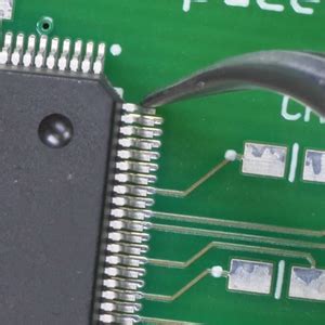
Despite taking all precautions, solder bridging may still occur on some QFPs after reflow. Removing these solder bridges is a delicate rework process.
For minor bridges between two leads, a soldering iron with a fine tip can often clear the bridge. Apply flux and gently drag the tip through the bridge to remove the excess solder. Do not apply excess heat or force, as this can damage the leads or lift pads.
Larger bridges or those spanning multiple leads require a solder wick. Solder wick is a fluxed copper braid that absorbs molten solder via capillary action. Place the wick over the bridge and apply the iron tip to heat the area. The solder bridge will melt and wick away from the leads.
A hot air rework station is often necessary for more extensive QFP bridging. Hot air reflow allows the entire QFP to be safely reflowed and the bridges to be cleared. Precise nozzle size and air temperature control is important to avoid overheating adjacent parts.
After reworking solder bridges, always inspect the QFP leads and solder joints for any signs of remaining defects. Many QFP solder joint defects are not visible to the naked eye. X-ray inspection provides a non-destructive method to verify joint integrity and locate hidden defects beneath the package.

Conclusion
QFP solder bridging is a challenging defect in PCB assembly, but it can be mitigated through proper process controls. Designing robust footprints and stencils, optimizing the printing and reflow profiles, and using undamaged components greatly reduces the occurrence of solder bridges.
When QFP bridges do occur, careful rework procedures can remove the defects and salvage the PCB. However, rework is time-consuming and runs the risk of damaging the board. Investing in process optimization and defect prevention is key to reducing rework and improving efficiency in QFP assembly.

FAQ
What is the most common cause of QFP solder bridges?
Excess solder paste printed on the PCB pads is the number one cause of QFP solder bridging. Applying too much paste causes solder balling and bridging between leads during reflow.
Can QFP solder bridges be prevented?
While QFP solder bridging can never be 100% eliminated, it can be minimized by following best practices. Optimal footprint and stencil design, precise paste printing, and a well-tuned reflow profile are all essential for preventing solder bridges.
How can solder paste inspection (SPI) prevent QFP bridging?
SPI systems use 2D and 3D imaging to measure solder paste print deposits. They provide real-time feedback on print volume, area, and alignment. This allows the printer settings to be adjusted to maintain optimal paste deposits and prevent overprinting that causes solder bridging.
What is the best method to rework QFP solder bridges?
For minor bridges between a few leads, a fine tipped soldering iron and solder wick can often remove the excess solder. More extensive bridging may require a hot air rework station to reflow the QFP. Always apply the minimum amount of heat necessary to clear the bridge.
How can x-ray inspection help identify QFP solder bridge defects?
X-ray inspection allows the assembled QFP solder joints to be viewed beneath the component body. It is effective for identifying solder bridges hidden under the QFP leads. X-ray can also reveal other defects such as voids, head-in-pillow, and insufficient solder fillets that are not visible from the exterior.


Leave a Reply