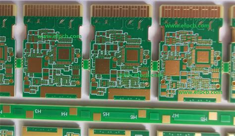
What is a Microvia PCB?
A microvia PCB is a printed circuit board that incorporates microvias – tiny holes that are less than 150 microns (μm) in diameter. These microvias enable high density interconnects between layers within the PCB. They allow for finer pitch components, reduced layer count, and smaller overall board size compared to traditional PCBs with larger through-hole vias.
Microvias are typically laser drilled and can be stacked or staggered across multiple layers to span a greater distance through the board. There are three main types of microvias based on the layers they connect:
| Microvia Type | Description |
|---|---|
| Blind Via | Connects an outer layer to an inner layer, but does not go through the entire board |
| Buried Via | Connects two or more inner layers but does not extend to either outer layer |
| Through Via | Goes through all layers of the board, connecting the top and bottom layers |
Using microvias allows designers to pack more functionality into smaller PCB footprints. This is especially advantageous for compact electronics devices like smartphones, wearables, and IoT products. However, the design and manufacturing processes for microvia PCBs are more complex and costly than standard PCBs.
Microvia PCB Design Considerations
Stack-up and Layer Count
The PCB Stack-up refers to the arrangement of copper and insulating layers that make up the board. With microvias, you can interconnect more layers within a thinner overall board thickness. This allows for higher wiring density and the ability to escape from fine-pitch BGA pads.
However, more layers also mean higher cost. So it’s important to use the minimum number of layers required for your design. Here are some general guidelines:
| Layer Count | Typical Applications |
|---|---|
| 4 | Simple designs, low-speed digital |
| 6-8 | Most digital designs, mixed-signal boards |
| 10-12 | High-density designs, high-speed digital, RF/microwave |
| 14+ | Extremely complex designs, high layer count packages |
Keep in mind that the stack-up configuration also affects signal integrity and power delivery. Work with your manufacturer to choose a stack-up that meets your electrical requirements and is cost-effective to fabricate.
Via Types and Placement
As mentioned earlier, there are three main types of microvias: blind, buried, and through. Each type has different design rules and cost implications.
Blind and buried vias require Sequential Lamination cycles during fabrication, which adds to the manufacturing cost and lead time. They also have limitations on aspect ratio (depth to diameter) and the number of layers that can be stacked. Through vias are the simplest and cheapest, but they consume more board real estate.
When placing vias in your design, consider the following:
- Use the largest via size that your design can accommodate to improve manufacturability and lower cost
- Follow the manufacturer’s guidelines for pad size, drill size, and annular ring
- Avoid placing vias under components unless absolutely necessary, as this can interfere with soldering
- Stagger vias to minimize stress on the board and prevent via-to-via shorting
- Use enough clearance between vias and traces to prevent manufacturing defects
Trace Width and Spacing
Microvia PCBs allow for finer trace widths and spacing compared to standard PCBs. This enables higher wiring density and the ability to route out of fine-pitch components.
However, thinner traces have higher resistance and are more susceptible to manufacturing defects. They also have lower current carrying capacity and may require more careful impedance control.
When designing traces, consider the following:
- Use the widest traces possible to minimize resistance and improve manufacturability
- Follow the manufacturer’s guidelines for minimum trace width and spacing based on the copper weight and layer
- Use thicker copper weights (1 oz or more) for high-current traces
- Perform impedance calculations to determine the trace width and spacing required for controlled impedance lines
- Keep trace lengths as short as possible to minimize signal loss and distortion
Component Placement and Routing
Microvia PCBs enable the use of smaller, finer-pitch components such as chip-scale packages (CSPs) and ball grid arrays (BGAs). However, these components can be more challenging to place and route.
When placing components, consider the following:
- Group related components together to minimize trace lengths and simplify routing
- Provide adequate clearance between components for assembly and rework
- Orient components to minimize crossing traces and vias
- Place decoupling capacitors as close to ICs as possible to minimize power supply noise
- Follow the manufacturer’s guidelines for pad size, shape, and spacing
When routing the board, consider the following:
- Route critical signals first, such as clocks, resets, and power supplies
- Minimize vias on high-speed signals to reduce discontinuities and reflections
- Use ground planes and power planes to provide low-impedance return paths and minimize crosstalk
- Avoid routing traces under components, as this can interfere with soldering and inspection
- Follow best practices for electromagnetic compatibility (EMC), such as avoiding routing near board edges and using guard traces

Microvia PCB Cost Considerations
Material Selection
The choice of PCB materials can have a significant impact on both performance and cost. For microvia PCBs, the most common materials are FR-4 and high-frequency laminates such as Rogers or Isola.
FR-4 is the most widely used and economical PCB material. It has good mechanical and thermal properties and is suitable for most digital and mixed-signal designs. However, it has higher dielectric loss and lower thermal conductivity compared to high-frequency laminates.
High-frequency laminates are engineered for low loss and high speed applications such as RF, microwave, and high-speed digital. They have lower dielectric constants and dissipation factors, which enable faster signal propagation and lower insertion loss. However, they are also more expensive and have different mechanical properties than FR-4.
When selecting materials, consider the following:
- Choose the lowest cost material that meets your electrical and mechanical requirements
- Use FR-4 for most digital and mixed-signal designs unless high frequency performance is critical
- Use high-frequency laminates for RF, microwave, and high-speed digital designs that require low loss and controlled impedance
- Consider the thermal conductivity and coefficient of thermal expansion (CTE) of the material, as this affects reliability and manufacturability
- Consult with your manufacturer to ensure the material is compatible with their processes and equipment
Manufacturing Process
The manufacturing process for microvia PCBs is more complex and costly than standard PCBs. This is due to the smaller feature sizes, tighter tolerances, and additional steps required.
The basic steps in the microvia PCB manufacturing process are:
- Drilling: Mechanical drilling of through holes and laser drilling of microvias
- Plating: Electroless copper plating followed by electrolytic copper plating to form the conductive layers
- Patterning: Application and exposure of photoresist, followed by etching to remove unwanted copper
- Lamination: Pressing the layers together with heat and pressure to form the multilayer board
- Solder mask: Application and patterning of solder mask to protect the copper traces
- Surface finish: Application of surface finish (e.g. ENIG, OSP) to protect the exposed copper and improve solderability
- Electrical test: Testing for opens, shorts, and other defects using automated equipment
Each of these steps has associated costs and yield losses that contribute to the overall manufacturing cost. In general, the more complex the design and the smaller the feature sizes, the higher the manufacturing cost.
To minimize manufacturing costs, consider the following:
- Use standard PCB materials and processes whenever possible
- Minimize the number of layers and microvia types used
- Use larger via sizes and trace widths to improve manufacturability
- Follow the manufacturer’s design rules and guidelines for feature sizes and spacing
- Use panelization to maximize material utilization and minimize handling
- Order in larger quantities to take advantage of volume discounts
Testing and Inspection
Microvia PCBs require more extensive testing and inspection than standard PCBs due to the smaller feature sizes and higher density. This includes both electrical testing and visual inspection.
Electrical testing typically involves flying probe or Bed-of-Nails Testing to check for opens, shorts, and other defects. The test coverage and pin count required depends on the complexity of the design and the reliability requirements.
Visual inspection is used to check for manufacturing defects such as misaligned holes, incorrect hole sizes, and incomplete plating. This can be done manually or using automated optical inspection (AOI) equipment.
To minimize testing and inspection costs, consider the following:
- Design for testability by providing test points and minimizing the number of buried vias
- Follow the manufacturer’s guidelines for test pad size and spacing
- Use boundary scan or built-in self-test (BIST) to minimize the need for external test equipment
- Specify the required test coverage and acceptance criteria upfront with the manufacturer
- Use statistical process control (SPC) to monitor and optimize the manufacturing process over time

Microvia PCB Design Tools and Resources
Designing microvia PCBs requires specialized tools and knowledge. Here are some of the key tools and resources available:
PCB Design Software
There are many PCB design software packages available that support microvia design. Some of the most popular include:
- Altium Designer
- Cadence Allegro
- Mentor Graphics PADS
- Eagle
- KiCad
These tools provide features such as schematic capture, layout, routing, and design rule checking (DRC). They also have libraries of components and footprints that can be customized for microvia designs.
When selecting PCB design software, consider the following:
- Ease of use and learning curve
- Support for microvia design rules and constraints
- Integration with simulation and analysis tools
- Compatibility with manufacturer’s data formats
- Cost and licensing model
Simulation and Analysis Tools
In addition to PCB design software, there are also specialized tools for simulating and analyzing microvia PCBs. These include:
- Signal integrity analysis tools (e.g. HyperLynx, Simbeor)
- Power integrity analysis tools (e.g. ANSYS SIwave, Cadence Sigrity)
- Electromagnetic simulation tools (e.g. HFSS, CST)
- Thermal analysis tools (e.g. FloTHERM, ANSYS Icepak)
These tools can help predict and optimize the electrical, thermal, and mechanical performance of the PCB before fabrication. They can also be used to troubleshoot issues and optimize the design iteratively.
Design Guidelines and Standards
There are several industry standards and guidelines that provide best practices for microvia PCB design. Some of the key ones include:
- IPC-2221: Generic Standard on Printed Board Design
- IPC-2226: Sectional Design Standard for High Density Interconnect (HDI) Printed Boards
- IPC-4761: Design Guide for Protection of Printed Board Via Structures
- IPC-6012: Qualification and Performance Specification for Rigid Printed Boards
- IPC-A-600: Acceptability of Printed Boards
These standards provide guidelines on topics such as via types and sizes, pad and antipad dimensions, copper foil thicknesses, and acceptability criteria for manufacturing defects.

Frequently Asked Questions (FAQ)
1. What is the minimum via size achievable with microvias?
The minimum via size depends on the PCB manufacturer’s capabilities and the number of layers to be interconnected. Typical minimum via sizes range from 50 μm to 100 μm in diameter, with aspect ratios of 0.5:1 to 1:1.
2. How many layers can be interconnected with microvias?
The number of layers that can be interconnected with microvias depends on the via type and the manufacturing process. Blind vias can typically interconnect 2-3 layers, while buried vias can interconnect 4-6 layers. Stacked Microvias can be used to span more layers, but this increases the manufacturing complexity and cost.
3. What is the cost impact of using microvias?
Using microvias typically increases the PCB Manufacturing Cost by 20-50% compared to standard through-hole vias. The cost impact depends on factors such as the number of layers, via density, and manufacturing process used. However, the higher cost can be offset by the ability to use smaller components, reduce layer count, and improve performance.
4. What are the reliability concerns with microvias?
The main reliability concerns with microvias are related to thermal and mechanical stress. Microvias have smaller cross-sectional areas and are more susceptible to cracking and delamination under thermal cycling and mechanical stress. This can be mitigated by using larger via sizes, adding support structures, and using materials with lower CTE mismatch.
5. What are the key challenges in microvia PCB design?
Some of the key challenges in microvia PCB design include:
- Managing signal integrity and power integrity in high-density designs
- Routing out of fine-pitch BGA and CSP components
- Controlling impedance and crosstalk in high-speed designs
- Optimizing via placement and stack-up for manufacturability and reliability
- Ensuring adequate test coverage and accessibility
- Managing the higher cost and lead time compared to standard PCBs
By understanding these challenges and using the right tools and techniques, designers can successfully create high-performance, cost-effective microvia PCBs.


Leave a Reply